TL;DR
If I were reborn as the Infra lead of some foundation-model team, I would certainly end up with all kinds of complaints about Nvidia's GPUs and the system as a whole, and then go build my own chip...
For Nvidia's networking part there is nothing to discuss: RoCE has all sorts of defects, and the DPU also comes with a pile of performance and security problems. No wonder Nvidia has started hyping Scale-in again this year, but for a team that has never run a cloud, it will take at least 5 more years to get mature in this area. As an example, we recently did something in our MaaS online business: in one PD-disaggregated scenario, simply replacing the transport protocol with CIPU's eRDMA cut TTFT by 40%, which is directly equivalent to saving a large number of Prefill compute servers while still holding the TTFT SLA...
On GPU microarchitecture, I wrote a detailed article about this last year, Inside Nvidia GPU: On the Shortcomings of Blackwell and a Prediction of Rubin's Microarchitecture (English version: https://github.com/zartbot/blog/issues/3 ), criticizing the various defects of Nvidia's Blackwell microarchitecture. Jensen even forwarded it internally at NV...
At the time I suggested that the SM should add a superscalar core for scheduling — and there you go, OpenAI's Jalapeño now has one. Another issue I have kept raising with Nvidia: in your GPU architecture, the large amount of L2 Cache takes up a lot of die area, yet it seems very hard to exert any control over it, the cache hierarchy is rather thick, and in order to maintain UMA you effectively add 200~400 cycles of latency across the two L2 Partitions; on top of that, external I/O interactions cannot be written directly into SMEM. Well, now it is settled — OpenAI's Jalapeño simply cut the L2 Cache out. And then there was the Anthropic interview problem I was grinding on a few months ago, which was in fact also preparation for tasks related to developing our own training and inference chips; I also wrote up a detailed internal analysis of various accelerator architectures and how it should be done...
In today's article analyzing Jalapeño, I will assume that I am the lead of foundation-model chip team, start from the model's requirements and the deficiencies of today's Nvidia GPUs, and derive step by step from first principles how it should be designed — and of course we will also gradually reproduce the entire design process inside the company. This is the way I will lay out Jalapeño's chip architecture and some of the toolchain behind it...
⚠️ A lot of the more detailed evaluation, as well as the work of reproducing the whole design flow, will not be made public...
1. Starting from Nvidia GPUs
The first thing that comes to mind is a joke — which is also the status quo.
- A product-management colleague: NV did it, so why don't we do it?
- Also a product-management colleague: NV hasn't even done it, so how could we do it?
- Still a product-management colleague: NV did it, so why do we still need to do it?
- And yet another product-management colleague: NV did it, so how would we dare to do it?
Most accelerator vendors have nothing on their minds but copying NV's homework, and then they give it the fine name of "CUDA ecosystem compatibility" — but no matter how they copy, they stay two to three generations behind NV overall... The other extreme is the constant urge to cook up some bizarre architecture in an attempt to overtake on the curve....
Yet the biggest gap between virtually all chip vendors and Nvidia lies in full-stack capability: from model structures and algorithms, to the software ecosystem, and finally to the chip implementation — where the trade-offs can be made, and what each trade wins and loses. Very few people can explain this clearly. As it happens, I understand the full stack from algorithms down to silicon, so I can lay out the entire chip design process, and the deficiencies of Nvidia GPUs, in full.
1.1 The Theoretical Peak in Inference Scenarios
GPUs have always processed large amounts of data with the mechanism of "hiding memory latency with a large number of concurrent warps", and this mechanism fundamentally relies on large batches. Once the batch gets small, there are few warps available to schedule, the pipeline cannot be filled, and you drift away from the roofline. This is exactly the problem so often encountered in inference scenarios: the latency-hiding mechanism breaks down.
Since the inference phase is to a large extent Memory bound, OpenAI did a very simple calculation. Assume the aggregate ScaleUP domain has N chips, each chip has HBM bandwidth M, and the model has a parameter scale of K; then, simply assuming compute is in no way a bottleneck, the theoretical maximum output token rate is
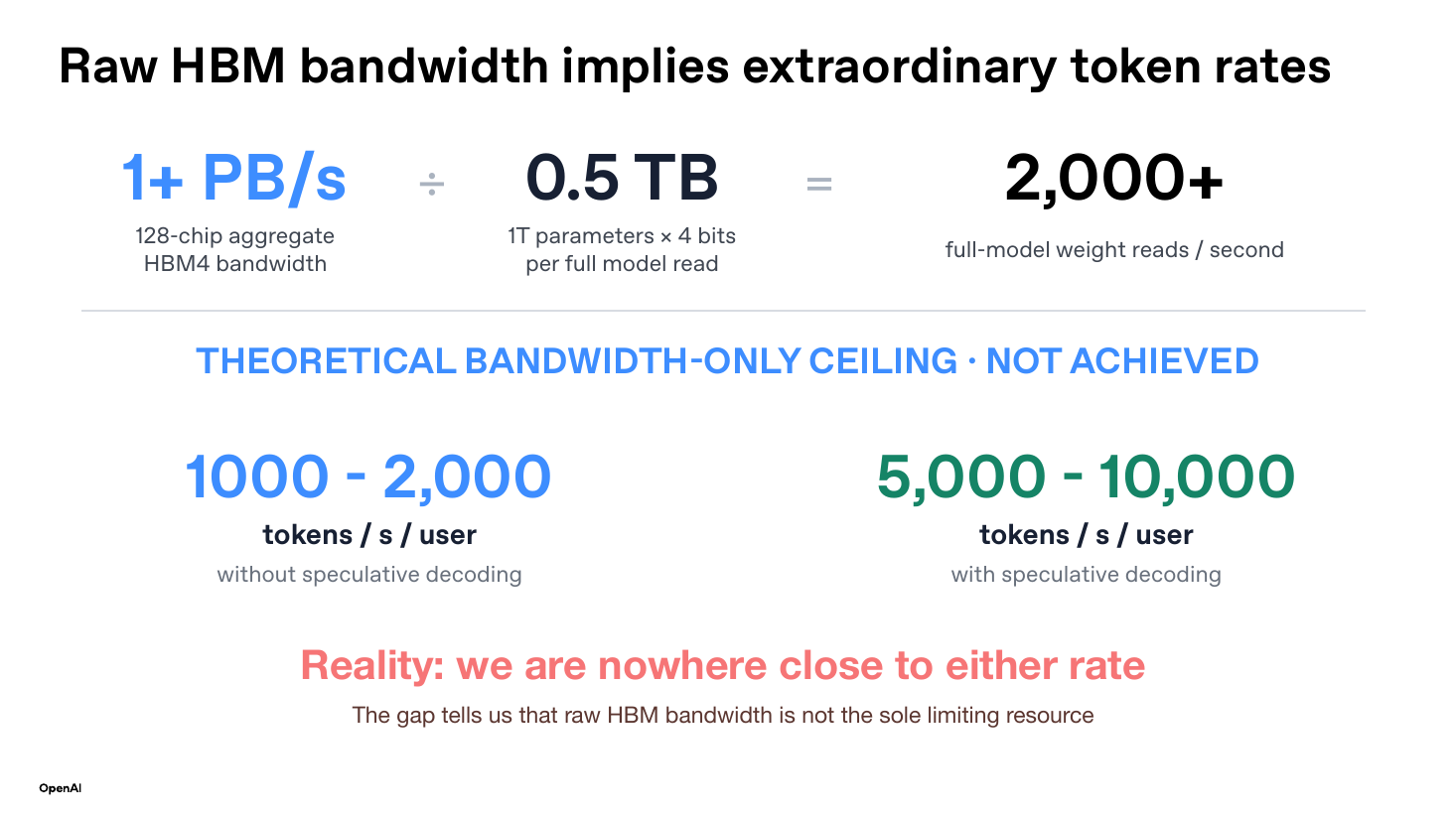
That is to say, in theory, without adding speculative decoding, a 1T-parameter model should be able to reach 1000~2000 tokens/s/user. But at this stage most inference frameworks on platforms such as the B300 can do at most 100~200 tokens/s/user — only 10% of the theoretical performance. So what this slide is saying is: even if you push HBM bandwidth to its theoretical limit, the resulting latency still has a lower bound. In other words, adding bandwidth alone cannot solve the low-latency problem. And since bandwidth is not the only variable, it must be an architectural problem...
1.2 Architecture Determines E2E Latency
In an article more than a year ago I hinted at this: looking at processors from the workload's point of view, in modern computer architecture the core design philosophy of the CPU is completely different from the GPU's. The GPU masks latency with massively parallel threads in order to maximize throughput, whereas the CPU spends an enormous budget of die area and transistor power without hesitation, exhausting every microarchitectural means available, to compress Single-Thread Latency to the absolute minimum.
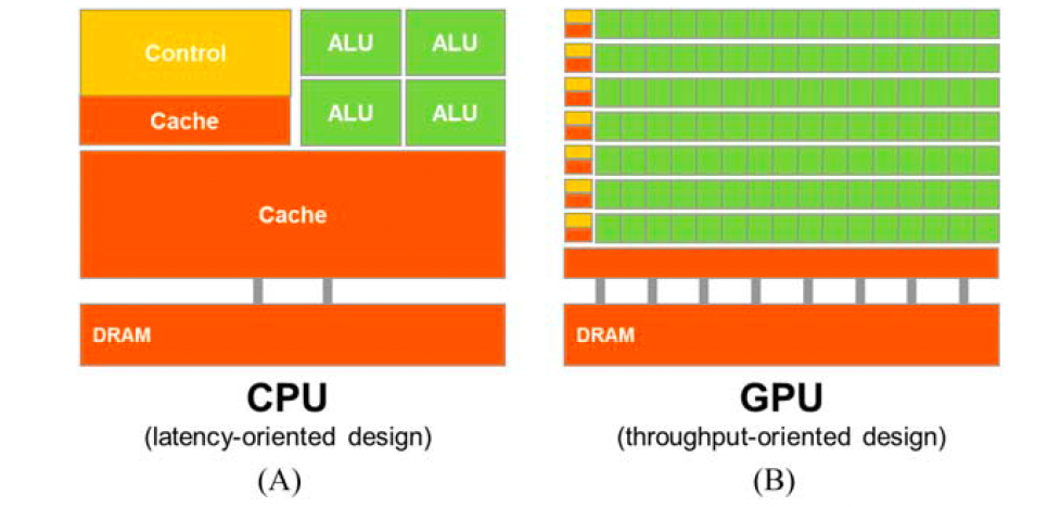
The CPU scouts ahead with branch prediction, squeezes parallel computation into every crack with multiple issue and out-of-order execution, pulls data closer with a multi-level cache hierarchy, and uses hardware cache coherence to achieve nanosecond-scale in-place data sharing among cores without memory synchronization — thereby masking the waiting latency of single-core computation, main-memory access, and multi-core cooperation.
By contrast, the GPU tilts the vast majority of its transistor budget toward dense arithmetic logic units, organizes tens of thousands of concurrent threads through the SIMT architecture, and relies on hardware-level ultra-fast thread context switching to instantly schedule other ready threads while some threads are waiting on memory. But it does not care in the least how fast or slow any single instruction is; instead it uses sheer parallelism to completely drown the overall processing latency of the data flow in a sea of compute tasks.
And for LLM inference, it falls exactly in the A* position in the table below. At batch=1 a single layer is just a few GEMVs, while at the same time you have to traverse dozens of layers within milliseconds, and also perform result synchronization after the large amount of parallel computation in the middle of every layer.
| Latency-sensitive | Latency-insensitive | |
|---|---|---|
| Large data scale | A* | GPU |
| Small data scale | CPU | NA |
OpenAI's session at HotChips also devoted a slide specifically to this problem: the latency we actually measure is to a large extent determined by the underlying architecture itself.
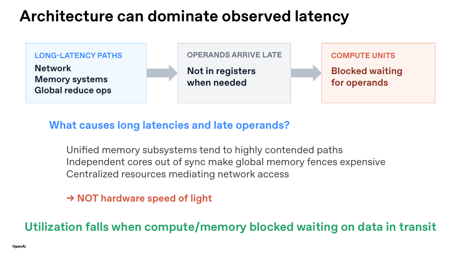
The long-latency path → operands arrive late → compute units stall in the figure adds another dimension to the traditional roofline model. For a GPU chip it is not simply a matter of classifying workloads as Compute bound or memory bound; you also have to add stalling, a state in which no resource is saturated and yet everything is waiting. Utilization drops while both ceilings are still far away.
1.3 The Deficiencies of Nvidia GPUs
In this section we will unfold OAI's slide in detail.
Let us first discuss the point OAI raised, Unified memory subsystems tend to highly contended paths. It adopts a unified L2 plus global addressing, so any core accesses any address equivalently. But although such unified access hides hardware complexity from the programmer, it also brings a large number of engineering constraints. For example, with too many SMs the bandwidth demand becomes too large, so starting from Ampere the L2 was split into 2 Partitions, and on Hopper a cross-partition access adds 200 cycles of latency. On Blackwell / Rubin the impact is even greater: each Die has two L2 partitions, so a Dual-Die part has 4 Partitions. On Blackwell this adds close to 400 cycles of latency; on Rubin you also have to consider that HBM4's aggregate bandwidth is already getting close to the L2 bandwidth, while additionally being subject to NV HBI. My personal view is that Unified Memory Access will make the actual utilization of HBM's 22TB/s only 60%~70%. And when concurrent requests exceed the port's service capability, the resulting Queuing Delay costs far more than the data transfer itself.
Another problem lies in data synchronization and warp scheduling. In modern GPU architectures every compute core has its own independent PC and advances asynchronously and freely, and combined with asynchronous memory-access engines such as TMA this increases throughput. But precisely because the compute cores are independent, the hardware cannot know in advance who will arrive when, so a global fence must genuinely "go around and ask everyone" — and for some operators it even requires a barrier across the entire system-level ScaleUP/ScaleOut network. This is what OAI referred to as Independent cores out of sync make global memory fences expensive.
Finally, Centralized resources mediating network access describes what happens when hundreds or thousands of cores need to initiate communication to an external network: if send and receive go through a centralized DMA controller, an MMIO interface, or a shared NIC port, the arbitration logic (Arbiter) becomes a severe throughput bottleneck and latency hotspot, completely dragging down the hardware's own blazing transfer capability. This touches on a whole series of complex interconnect-system problems; NOC / ScaleUP / ScaleOut all have their own issues — for example the CopyEngine used when copying KVCache, or the doorbell constraints on the ScaleOut NIC, plus the fact that many notifications cannot be written directly into SMEM, so they can only be written to some Remote GMEM and then have the CUDA Core poll GMEM.
It is precisely for these reasons that over the past few years I kept proposing to Nvidia that the SM needs a superscalar core so that the programmer can better control instruction issue and scheduling, and that at the same time the user should be given more control over L2 and it should be further fused with the SMEM inside the SM... And as it happens, OpenAI's Jalapeño made exactly these choices. In the next chapter we will gradually unfold, from the first principles of the inference business, how to design a chip suited to inference.
2. How to Design an Inference Chip
When we analyze carefully, we find that the deficiencies described in the previous section are all the price of generality. It needs to be emphasized that this is not saying the GPGPU is badly designed, because every one of those decisions was right at the time — it is the key to Nvidia's success, and the CUDA SIMT programming paradigm enormously simplified the complexity of writing parallel programs for everyone over the past decade or more. But this premise brings a large number of problems in the LLM inference scenario, and then, along with the development of Coding Agents, all kinds of Auto-Kernel work (e.g. KDA) is blossoming, so it seems we no longer need to pay such a high price for that generality...
But all of this is only from the chip-architecture point of view. More importantly, we need to take the perspective of the inference business as a whole as our first principle.
2.1 First Principles of an Inference Chip
From first principles, from the point of view of operating an inference service, it mainly comes down to outputting as many tokens as possible while meeting the user experience SLO under the constraints of infrastructure cost and supply-chain constraints. And in North America the biggest supply-chain constraint is probably mainly power supply.
This is why OpenAI's presentation deliberately does not list chips used, throughput per chip, or TTFT as primary objectives. What it chooses instead is request-level user experience and energy per request.
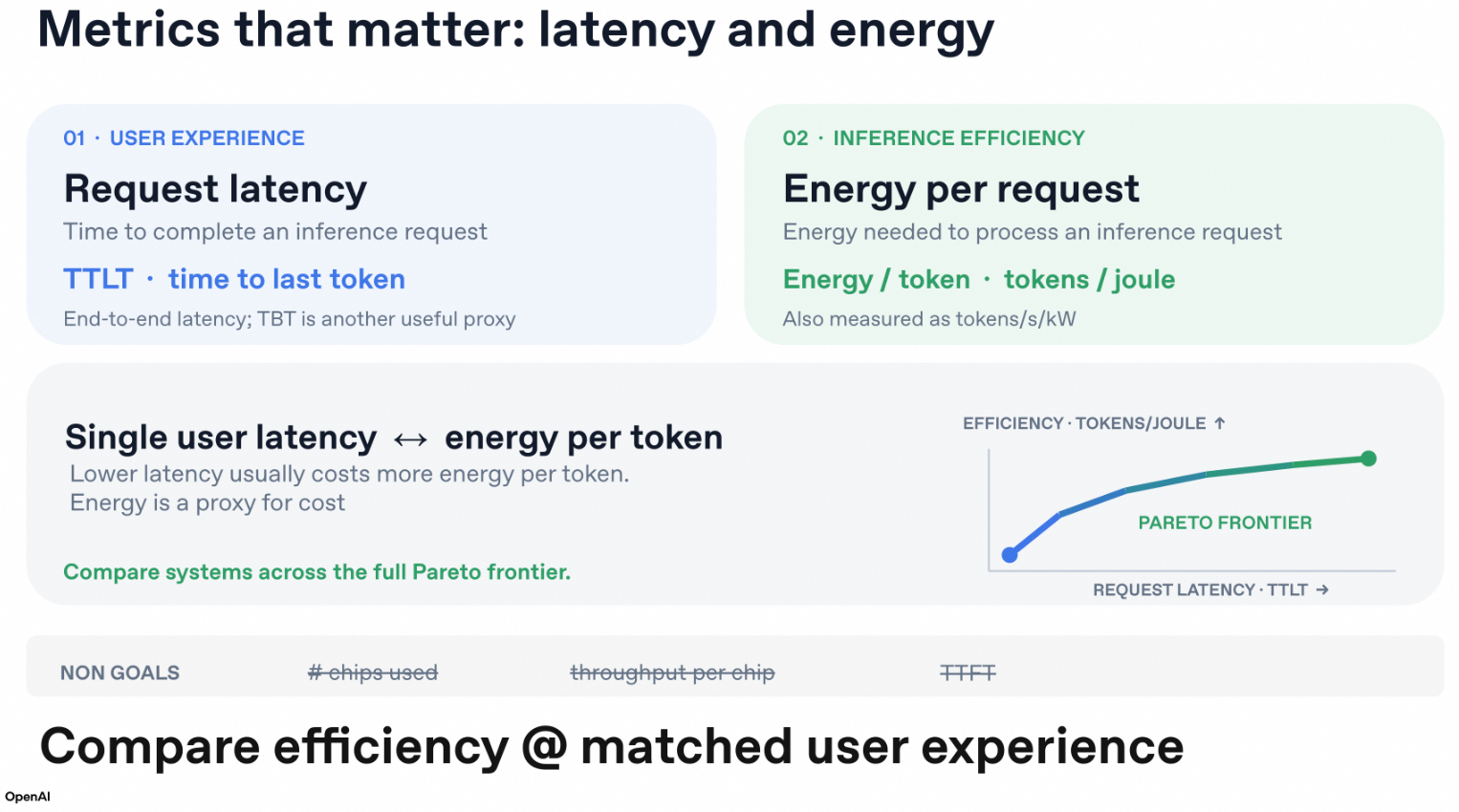
Throughput can mask certain waits through concurrency, but the dependency chain of a single task cannot be parallelized out of thin air. Hence the use of TTLT, i.e. time to last token, to represent the completion time of the whole request, together with TBT, i.e. time between tokens, to approximate the streaming interaction speed. But we note that lowering the batch usually improves TBT, yet it reduces weight and network reuse and raises the energy per token. Raising the batch usually improves tokens/s/kW, but request queuing and the per-user inter-token interval get longer. There is therefore a Pareto frontier between response latency (TTLT) and energy efficiency (tokens/Joule). Formally:
And LLM inference is, in fact, the single-thread latency problem that the CPU world has been researching for thirty years...
| The CPU world's answer | Its counterpart in LLM inference |
|---|---|
| Branch prediction: guess the next step, roll back if wrong | Speculative decoding: guess the next tokens, discard if wrong |
| Out-of-order execution: find independent work in the gaps of the dependency chain | Out-of-order core |
| Cache + prefetch: move latency off the critical path | A hardware-managed L1 + well-behaved prefetch, rather than scratchpad + DMA |
| SMT: fill the gap with another thread | Fill the gap with another sequence (request-level batching) |
| Widening the issue width has diminishing returns (the ILP ceiling) | Increasing speculation depth has diminishing returns (the acceptance-rate ceiling) |
From the architectural point of view, then, we arrive at a very simple conclusion:
- Maximize Data Locality and reduce the cost of data movement.
- From the E2E latency point of view, further increase the parallelism of instruction execution and reduce idle waiting time.
In the next few subsections we will unfold a detailed analysis from the technical details of inference...
2.2 The Current State of Inference Infra
2.2.1 Performance Requirements of the Different Phases
For an inference system in general, the main workload splits into three parts, Prefill, Decode, and SpecDecode. Our original qualitative conclusion may have been that Prefill is Compute Bound and Decode is Memory Bound, but in reality, from the E2E latency point of view, we also need to consider the two phases of SpecDecode — the Draft model and Verify — which sit at different positions on the roofline.
OpenAI also discussed this problem in its hotchips session, but its formulation is incomplete. For example, in the third panel the main title is Spec-verify and the subtitle is Decode; yet autoregressive decode with and batched verify with sit at two different positions on the roofline, differing by a factor of in arithmetic intensity.
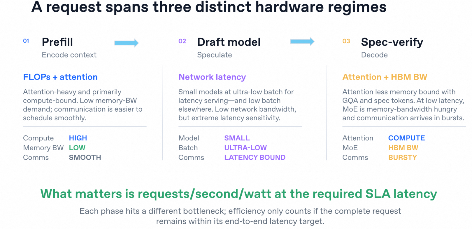
We therefore strictly split it into four parts, and to simplify the problem under analysis, we analyze it here in terms of processing a single Request
1. Prefill: Prefill processes the complete input context in one pass. For an ordinary Transformer model with hidden-dim and length , the main compute of the projections and the FFN grows roughly as , and the score part of full attention grows as . A large provides a sufficient M dimension, and the weights can be reused across many tokens, so the tensor engine easily enters the high-utilization region. It is therefore a Compute-bound computation, i.e. compute high, memory BW low. As for communication, its collective messages grow as , making it bandwidth-limited rather than latency-limited, and hence easy to schedule smoothly.
2. Decode: In the Decode phase an autoregressive model processes only 1 new token per sequence per step, i.e. , and the matrix computation degenerates into a GEMV. This means one copy of the weights serves only one row, so at short or moderate context it is usually limited by Weight HBM bandwidth, and at long context it gradually shifts to being limited by KVCache HBM bandwidth. In a distributed system, meanwhile, every layer boundary still has to perform one collective, and the message is only in size, so the network synchronization latency of small-message collectives may become the primary bottleneck.
3. Draft Model: This is usually model-dependent. Classic autoregressive draft models and EAGLE-style methods need to execute multiple serial drafting steps, and are therefore frequently limited by weight/KVCache bandwidth and synchronization latency. DFlash uses a single block-parallel diffusion backbone forward pass to generate the entire draft block at once. DSpark uses a single parallel backbone forward pass and then layers on a low-cost Markov or RNN serial head. For DFlash/DSpark, the draft weights only need to be read once per backbone invocation, the arithmetic intensity can rise with , and the bottleneck may shift to matrix compute, target hidden-feature/KV injection bandwidth, vocabulary projection, or the lightweight serial sampling latency.
4. Verify: The number of physical tokens verified is also not necessarily equal to a fixed . Linear drafts usually verify one prefix, tree drafts need to verify all tree nodes, and DSpark selects a different verification length for each request according to confidence and real-time hardware capacity. Dense weights can be reused across the physical verification tokens of the current round, but a MoE target model may lose most of its weight reuse because the deduplicated expert count grows with the token budget. Efficient verification attention must let one prefix KV block be reused by all candidate queries or tree nodes of the same request.
Summarized into a table:
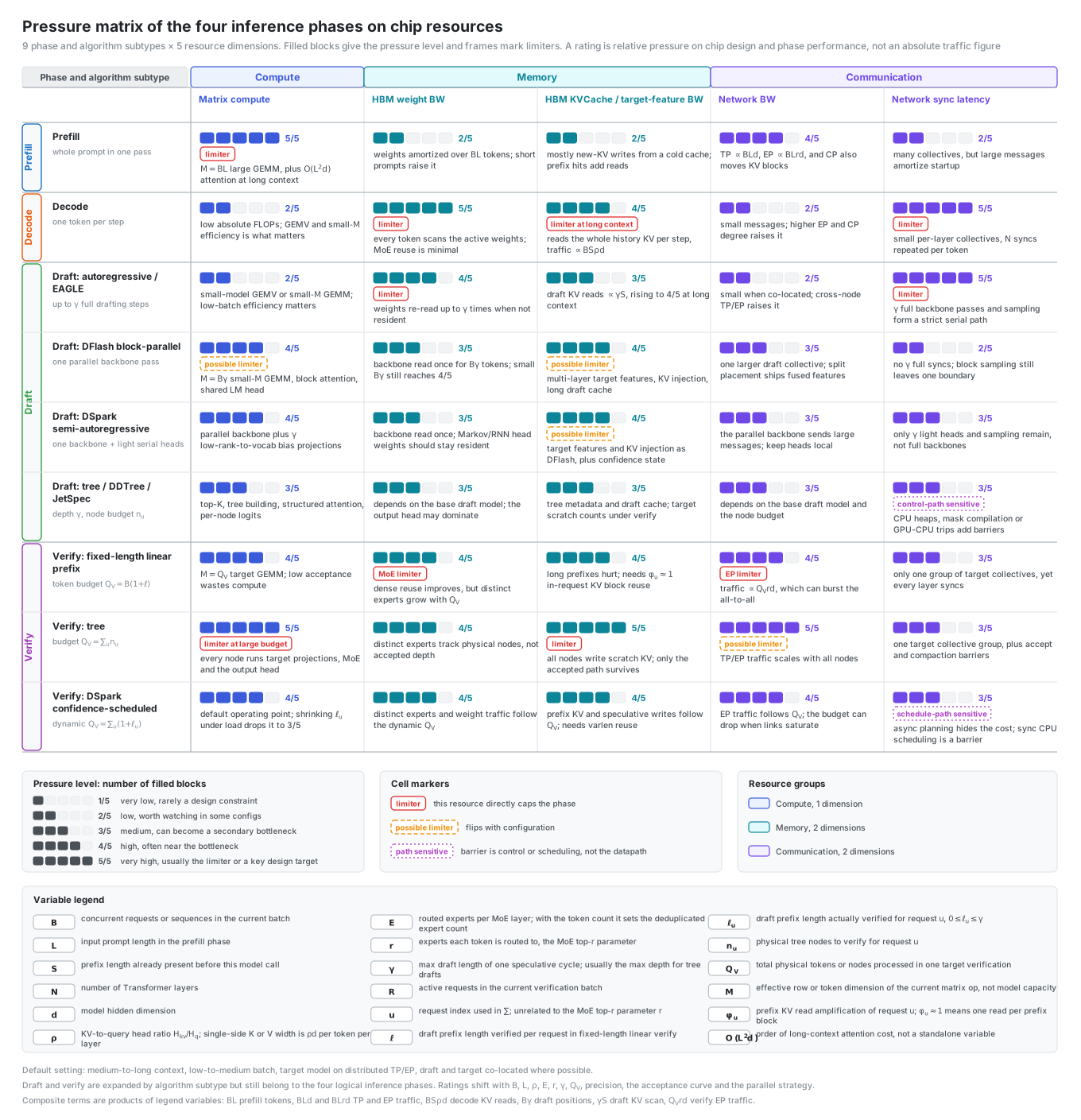
As you can see, the demands the different phases place on the chip's compute, memory, network bandwidth, and network synchronization latency differ enormously. If we use a dedicated chip for each phase, the resource ratios also become a problem. OpenAI discussed this too:
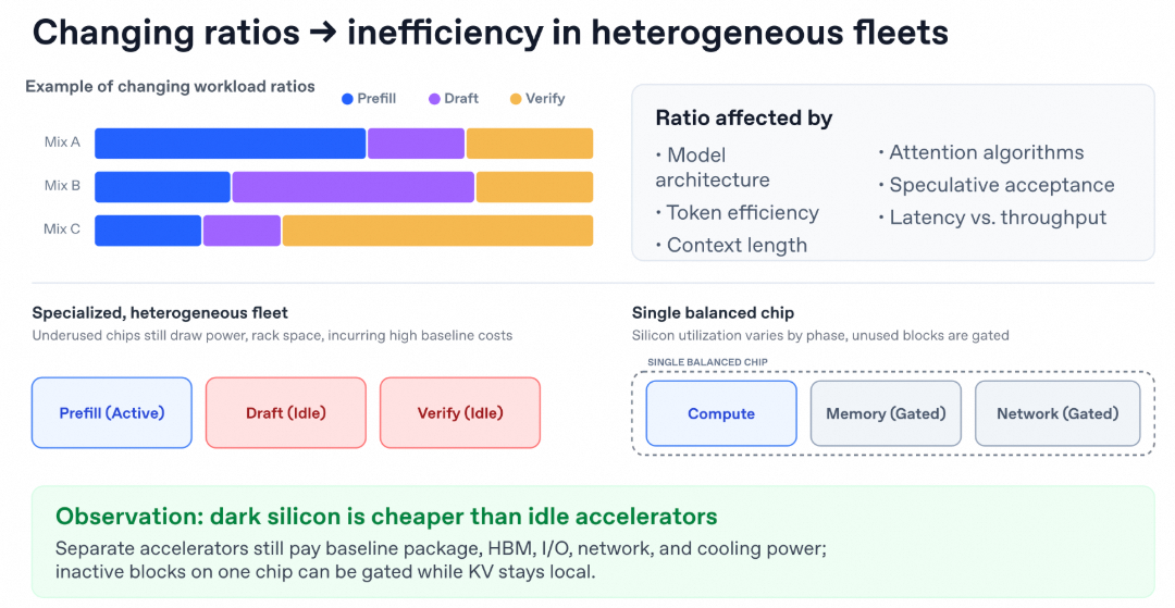
What OAI lays out is the deficiency of today's LPU-style deployments such as the various PD-disaggregated and AFD/SpecDecode schemes. The original slide sticks to its own three-way split, so it only draws the three ratios prefill, draft, verify. In reality, putting the 4 phases we distinguished earlier into 4 kinds of dedicated devices appears to let every chip be optimal for its own kernels. The problem is that the number of devices is discrete and relatively fixed once deployed. Let the capability of the 4 pools be and the arriving workload be , with the subscript corresponding in order to prefill, decode, speculate and verify; then the serviceable rate is limited by the most strained pool:
As an example, let us analyze the effect of the SpecDecode acceptance rate changing dynamically. and rise and fall at each other's expense, and what moves them is not the requests. An output token of a request has only two ways out: pure decode, or Draft + Verify. Let be the fraction of output tokens committed through the SpecDecode path, and the number of committed output tokens per second; then
where is the cost of one Draft Model round — steps for autoregressive, 1 wide pass for block-parallel — and is proportional to that round's physical token budget. is not determined by the request mix: an collapse pushes it toward 0; under high concurrency, the scheduler trimming low-confidence suffixes by prefix survival probability also pushes it toward 0; and when the acceptance rate recovers, it goes back to 1.
So with the same batch of requests, the same model, and the same context length, the load of the decode pool and that of the verify pool can head to two opposite extremes. The decode pool must be provisioned for and the draft and verify pools must be provisioned for , and these two peaks do not arrive at the same time: what you reserve is the sum of the peaks, what you use is one of the groups.
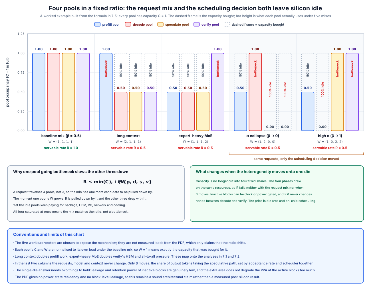
The limiting term of the four phases falls on a different resource axis in each case: prefill is matrix compute, decode is HBM weight bandwidth plus per-layer synchronization latency, autoregressive drafting is draft weight bandwidth plus synchronizations, and verify is the weight traffic of deduplicated experts plus EP all-to-all bursts. So these four dedicated chips are not large and small versions of the same chip, but four different chips whose ratios of compute, bandwidth and network differ from one another. When the acceptance rate rises, the number of verifies falls; when the context length rises, the cost of prefill and KV goes up; when the model is swapped for a MoE with a high expert fraction, the network and HBM pressure of verify goes up again. When one pool becomes the bottleneck, the other two still have to pay the baseline cost of package, HBM, I/O, network and cooling.
This leads to a consequence that is easy to miss: even if operations were willing to move devices from an idle pool into the bottleneck pool, they would be unusable once moved, because a prefill chip's HBM-to-compute ratio was never provisioned for decode in the first place. A fixed ratio of device counts is equivalent to locking down five resource-dimension ratios at the same time.
2.2.2 The Cost of KVCache
In traditional inference deployments we usually consider a PD-disaggregated deployment, and in that case the movement of large amounts of KVCache also brings enormous power consumption and network synchronization losses. OpenAI's exposition at hotchips is as follows:
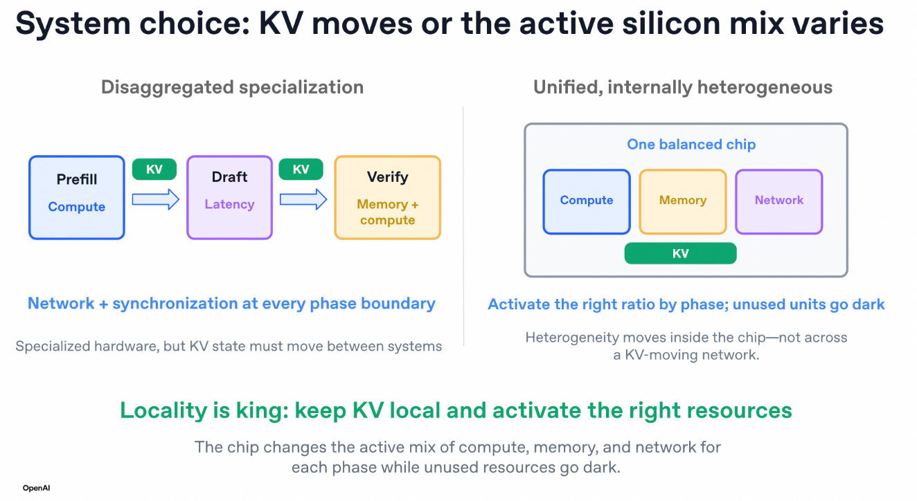
This slide compresses the architectural choice into a binary: either heterogeneity happens between systems, at the cost of the KV following the different phases around — which is exactly today's PD-disaggregated approach, but the impact of each phase's network and synchronization plus the power consumption of moving KVCache is enormous. The other choice is to put the KVCache movement between different phases inside the chip, at the cost of the ratio of active resources changing with the phases.
The size of the KVCache is typically , proportional to the sequence length, and even some Linear Attention algorithms need to leave a Snapshot behind for each round across multiple interactions. Moving the data affects the performance of the existing collective communication over ScaleUP/ScaleOut as well as the NOC; at the same time you also have to consider that reading large amounts of KVCache out of the Prefill node's HBM and then writing it into the Decode node's HBM still affects the execution of the original inference operators. A concrete analysis can be unfolded quantitatively along four directions: time ratio, per-round boundary, HBM capacity, and transaction semantics.
Because this part is confidential I will not say much more publicly...Remember what I said at the beginning of this article: after our MaaS service switched the transport protocol to CIPU eRDMA, TTFT dropped by 40% without a single line of code changed in the inference engine...
Finally, as for the chip design, if you use several independent accelerators, the KV cache has to move between devices. Jalapeño's strategy is to put the heterogeneous capability inside one balanced chip:
- When the current phase needs tensor compute, activate more compute units.
- When the current phase is HBM-limited, emphasize the local memory path.
- When the current phase is communication-intensive, use the collective and scale-up networks.
- Power-gate the modules that are not needed for the moment.
- Keep the KV cache local as much as possible.
2.3 Inference Chip Architecture
A few months ago David Patterson published an article, *Challenges and Research Directions for Large Language Model Inference Hardware*[1], laying out the architecture of inference hardware. On the memory subsystem there is a great deal of discussion of using HBM / 3D-DRAM / HBF, but in order to simplify the problem — for example, new HBM can build PNM and a Customized Base Die that moves the Memory Controller and HBM PHY out of the compute Die to gain more compute resources, or one can use 3D packaging of XCD and FCD as AMD does, which can further improve XCD yield and allow a larger L2 Cache and interconnect NOC — we will set that part aside for now and focus more on the microarchitecture inside the compute Die and on the interconnect architecture.
Internally in the company there is also a detailed document analyzing the microarchitecture of various compute chips, including Nvidia GPGPU / LPU / Google TPU and Huawei Ascend 950, along with a series of explorations of Agent based compiler work.
2.3.1 Changes in the Programming Interface
A few months ago I was working on a performance-engineering take-home interview problem used for hiring at Anthropic; the task code is at https://github.com/anthropics/original_performance_takehome. Roughly speaking, it is about performance optimization on a custom VLIW + SIMD processor. Optimizing with the Claude-Opus model, I climbed to second place, and then since the gap was already within 2%, plus some compute-resource and token-cost considerations, I stopped there — apparently I am still third...
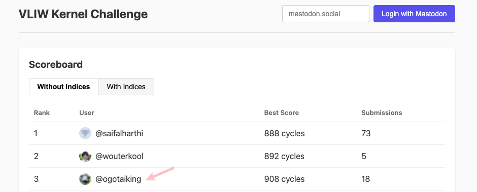
This problem made me realize that it is precisely about designing the compilation system of a dedicated ASIC chip for inference and training. It seems that although the existing CUDA ecosystem and the SIMT programming interface are friendly to humans, the resource overhead they bring is enormous; yet now that we have Agent as compiler, and along with work like Ligeng's KDA, kernel optimization seems to be something an Agent can do quite well, so it seems we never again need to accommodate the cognitive limitations of humans, and can instead exploit the hardware's capability to the fullest.
In that case the original SIMT abstraction, and the GPGPU's advantage in inference scenarios, no longer hold. Typically a model's architecture is already frozen during the pre-training phase, so we will have two months to thoroughly tune the inference platform with Agents. This is also a shackle that OpenAI's Jalapeño architecture has released.
2.3.2 Architectural Trade-offs
Last year's blog also discussed one issue: Nvidia's warp scheduling mechanism and latency-hiding mechanism are not a good fit for inference scenarios. On another front, the article On GPU Memory Models and Interconnect Network Design also discussed the complex memory semantics of the Nvidia GPGPU: there is a Generic Proxy and an Async Proxy on the data path, and if you need ScaleOut you also need an extra synchronization mechanism; then the whole NOC and memory hierarchy keeps getting heavier, and looking at the warp scheduling mechanism, it does not satisfy me — every data movement has to be explicitly orchestrated, and the orchestration itself has overhead: constructing the DMA descriptor, launching it, and the barrier waiting for completion, and so on...
Suppose computing one tile takes only 500 cycles while the DMA orchestration + barrier overhead is 100 cycles; then the fixed overhead accounts for 20%. But in the typical GPU/TPU scenario (large batch, a tile takes a few thousand cycles) the same 100 cycles account for only 2%, entirely negligible. Unfortunately, the Decode phase falls exactly into the former case: the batch is small and the compute per tile is small, so the synchronization overhead goes from "negligible" to "dominant". At that point switching synchronization from an "explicit barrier" to "hardware dependency tracking (out-of-order + cache)" has a positive payoff.
Therefore, I hoped they would add a superscalar core inside the SM to further control latency — and it happens that the Out-of-Order Core in OpenAI's Jalapeño confirms this judgment.
At the same time, some while ago I also carried out complete cycle-level instruction measurements and full chip-level analysis of the Blackwell family, published publicly as *Dissecting SM_120 through Microbenchmarking*[2]. And on the B300's on-chip network / L2 Cache and power management we also found a large number of problems. In short, the whole memory hierarchy is too heavy, and in the on-chip network, in order to sustain L2 bandwidth, it was designed as 2 Partitions very early on. Nvidia hopes to keep maintaining the UMA programming model to hide the latency difference between accesses to the different L2 Partitions, but on multi-die Blackwell / Rubin the price is too high: the multi-die structure gives a single GPU 4 L2 Partitions, and maintaining UMA on top of that introduces as much as several hundred cycles of memory-access loss in the inference phase, which is clearly not worth it.
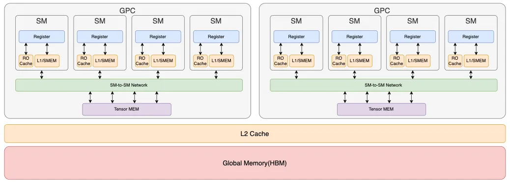
On another front, in scenarios such as RDMA, I would like many notification mechanisms to be able to bypass L2 and write directly into SMEM, so that the SM can poll SMEM very quickly and obtain relatively deterministic latency; whereas polling GMEM today may well get the warp yielded by the warp scheduler, resulting in even greater latency. Moreover, the L2 Cache mechanism is very hard for us to control: it is quite possible that some of our critical synchronization counters get evicted by the SMs' massive memory accesses. I have also kept asking Nvidia when they will be able to carve out part of the L2 Cache as something user-controllable like SMEM....
There are further problems as well. For instance, because of the impact of the synchronization mechanism, the performance of collective communication, whether intra-chip or inter-chip, is affected by latency, and this is also why in many scenarios the scale of TP parallelism cannot be scaled further, which becomes a significant limiting factor. And these problems all seem to come from the effects of UMA, so a very natural idea is: could we make it a NUMA structure, and fully optimize the critical collective-communication-related processing in the NOC and the interconnect (ScaleUP/Scale Out)?
Of course I can understand why Nvidia, as a commercial company, has to chase peak throughput. But for an inference system, starting from the objective function, we have two independent corollaries, landing respectively on the microarchitecture and the system architecture.
Corollary A: Effective tokens must be obtained through "high utilization at low latency", not by piling on batch. Concretely:
- Shorten the memory access path: give up the strategy of hiding memory latency, and instead eliminate it through fewer memory levels; the price of NUMA is acceptable
- Higher ILP within a single instruction stream: use an out-of-order core + hardware L1 + prefetch, rather than relying on occupancy
- An appropriate matrix unit size: guarantee there is no performance loss at small batch as well
- Eliminate the fixed overhead of kernel launch and synchronization
Corollary B: Die area is no longer the scarce resource; an idle machine is the real waste.
- Reject the various disaggregation techniques of heterogeneity; a homogeneous cluster avoids the scheduling bottleneck of dedicated resources
- Do not target peak FLOPS; fully account for the resource requirements of each inference phase and achieve a balance of compute / memory bandwidth / communication
- Allow a certain amount of dark silicon to guarantee the chip meets the requirements of every phase
- Balance the power of the whole chip, and take that as the chip's design objective
- Reduce communication latency, especially tail latency
The whole set of architectural decisions can be summarized in the figure below:
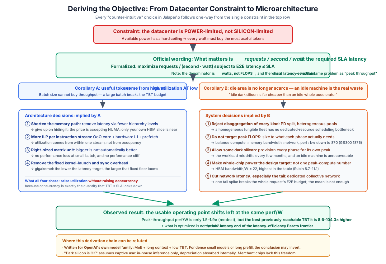
And these architectural considerations happen to coincide with OpenAI's. We will unfold the concrete analysis in the next chapter.
3. The OpenAI Jalapeño Chip Architecture
Jalapeño should be the industry's first hardware/software co-designed chip platform for AI acceleration. On the hardware side it took only 9 months from the first line of RTL to final tapeout, which of course is also closely tied to the overall chip architecture: because there is no complex synchronization or hardware scheduling mechanism, the verification cycle was sped up a great deal.
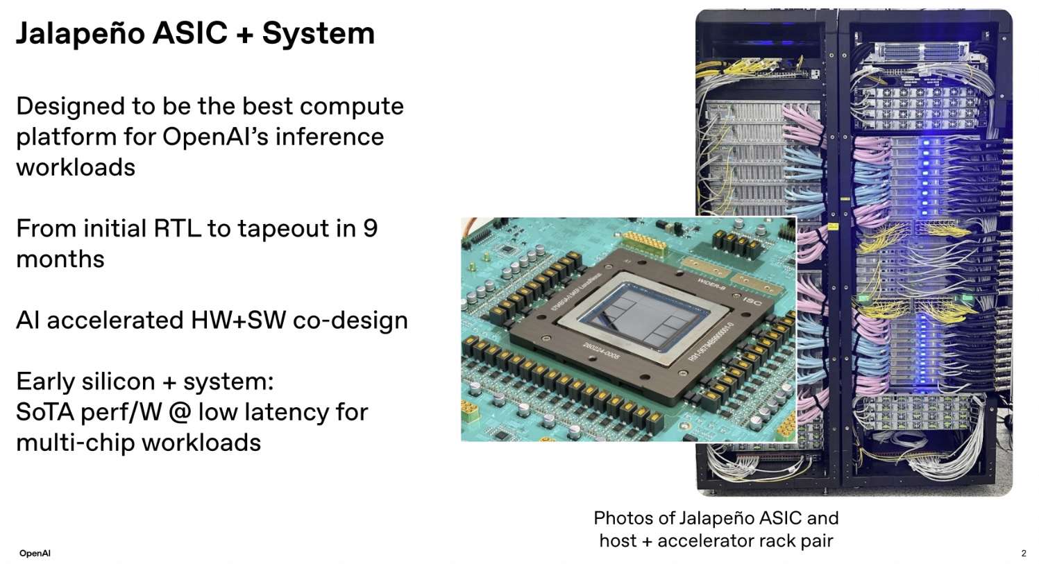
Also, for time-to-market, the whole chip reuses a relatively mature Ethernet based Scale-UP. The industry's very first ScaleUP with memory semantics built on standard Ethernet should be NetDAM, which I developed in 2020; this is likewise a very simple engineering trade-off — the supply chain for commodity switch chips is excellent and the cost is very low, even though there are still some deficiencies in latency and effective utilization. But for the extremely low-latency interconnect that an inference chip needs, this is only a temporary solution. Even the SUE that BRCM later introduced has fairly large deficiencies; in the course of talking with them, I told them they could look at some of FinePack's approaches, but in the end I found that BRCM does not have the complete knowledge background and had not accounted for some very fine-grained queuing delays, in particular the suppression of certain tail latencies...
3.1 Chip Architecture Overview
Jalapeño's chip architecture is shown in the figure below:
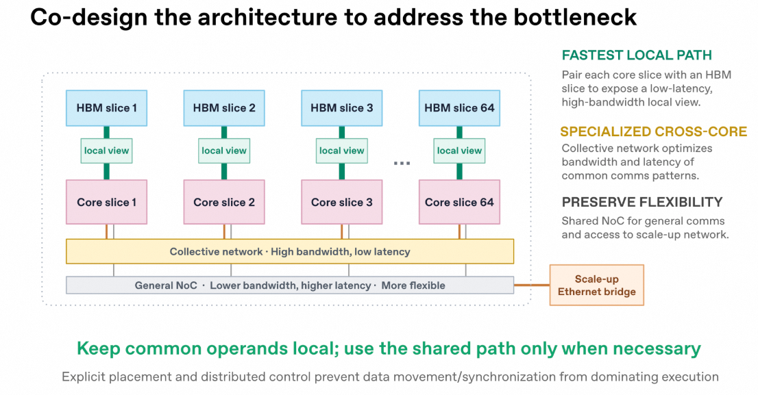
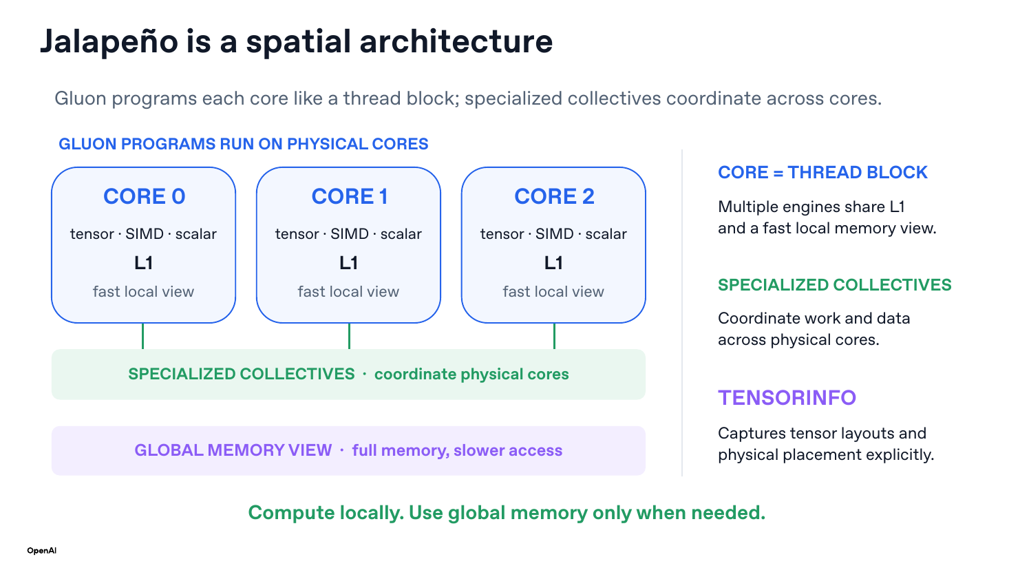
It abandons the Nvidia-style UMA structure and instead pairs compute cores with HBM Slices one-to-one, building the lowest-latency memory access path. The on-chip network is then specially optimized for low latency and high bandwidth for cross-die collective communication. And it also keeps a fallback ScaleUP interconnect path based on commodity Ethernet.
Such a design is likewise the result of hardware/software co-design: many of Jalapeño's hardware simplifications (removing the unified L2, giving up cross-card memory semantics, exposing NUMA distance) push the complexity onto the compiler and the kernels. Note the sentence at the bottom — it essentially means that through explicit placement, which slice the data lands in is deliberately arranged, and good optimizations are built through the compiler; we will unfold this in detail later in the software system architecture. At the same time, the chip has no central scheduler: every core fetches and advances independently, and the benefit of this is to prevent "data movement and synchronization" from dominating execution time.
The whole chip uses a multi-Die package, as shown below:
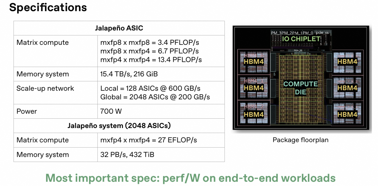
The Compute Die is built in TSMC N3P and basically maxes out the reticle size; total compute reaches 13.4 PFLOPS at MXFP4, and it attaches 6 HBM4 stacks. But the IO is split out into a separate IO-Die, built in TSMC N3E. Decoupling IO from compute means the next generation can swap only the compute die and reuse the IO chiplet, or vice versa, and it also reduces the resource footprint on the Compute Die. For a project that is just starting out and needs to iterate fast, this is a valuable degree of freedom. Also, the ScaleUP as a whole does not chase maximum bandwidth to the extreme, supporting only 600GB/s local (in-rack) and 200GB/s global (cross-rack).
We also note that its Matrix engine natively supports MXFP8 × MXFP4, which is the activation-FP8 × weight-FP4 path commonly used in MoE; in addition, the chip as a whole should still have BF16 support for attention computation.
3.1.1 Core Slice Architecture
From the publicly known information, we speculate that its compute core structure is as follows:
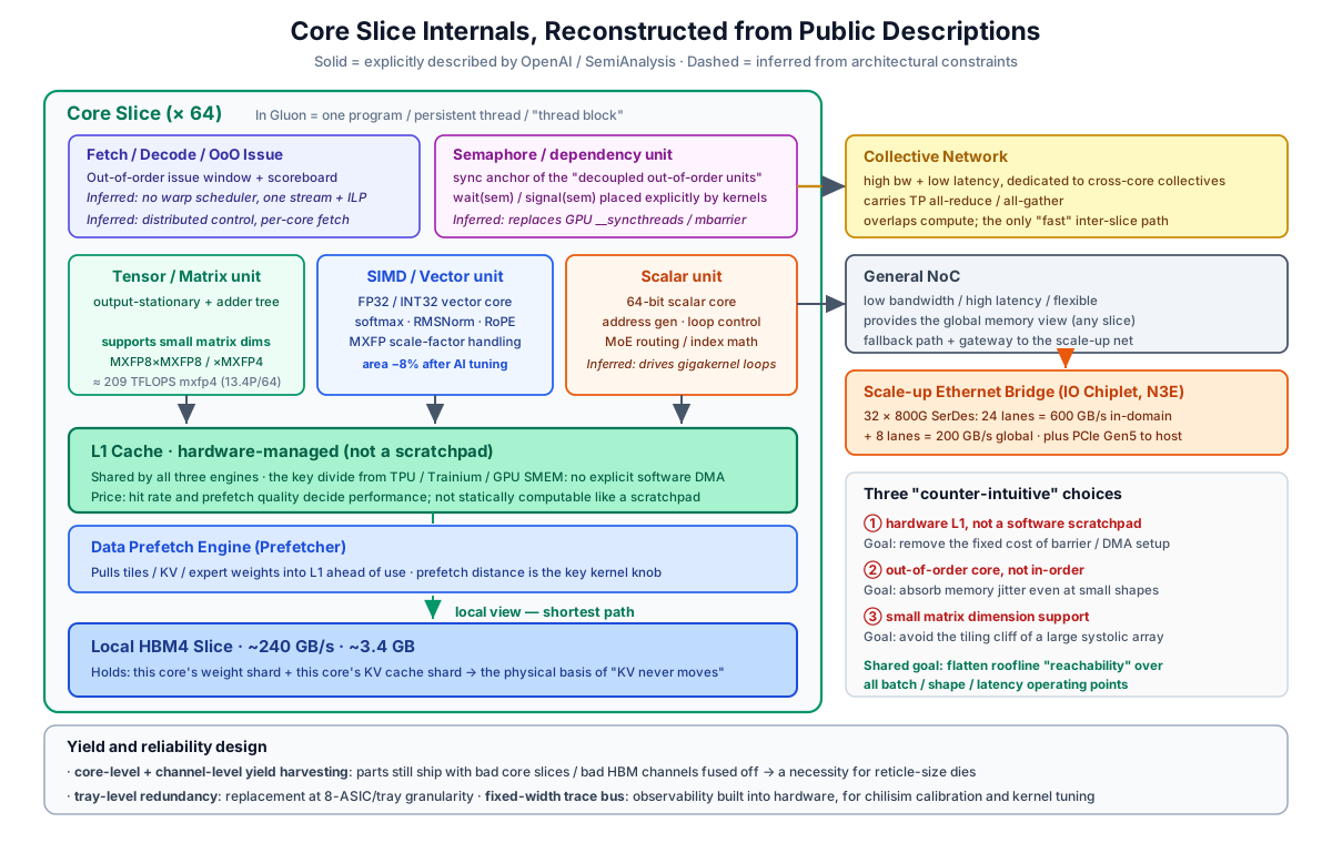
First, the entire program executes as one GigaKernel, similar to a Persistent Kernel in CUDA. But since Jalapeño has to care much more about latency, there will be no situation like CUDA Cores with many warps resident; instead it relies more on the prefetch and out-of-order window inside a single instruction stream, built by the internal superscalar structure, to hide latency — this is where its front-end fetch / decode / out-of-order issue come from. To keep the whole core running at high performance, there should be a relatively independent synchronization anchor performing capabilities similar to __syncthreads / mbarrier in a GPU.
Then in the compute units, it is generally the standard composition of a Tensor/Matrix Unit, a SIMD/Vector Unit and a Scalar Unit. The most critical part is the architecture of the Matrix Unit. We expect it to achieve higher utilization at the small batches of inference Decode, while overall also satisfying compute-bound computation such as Prefill. And this is the single most critical link of the whole chip: how does it cooperate with out-of-order execution? What is the optimal Shape? How is latency hidden? We will unfold this in detail in a later section.
Next is the memory subsystem. It is not configured like Nvidia's SM with a RegisterFile / L1Cache / SMEM / TMEM; there is only an L1 Cache, and the whole chip likewise has no global L2 Cache. HBM is then sliced and attached directly to each Core Slice, which nicely avoids contention on the NOC.
The biggest difference from Nvidia is that between its Tensor Unit and its SIMD Unit / Scalar Unit there is no need to frequently move and copy data among SMEM / TMEM, the Register File, and the L1 Cache. The Tensor Unit and the SIMD Unit share operands directly through the L1 Cache, and once the Tensor Unit finishes computing, a SIMD instruction can be issued immediately to continue computing. This eliminates fixed overheads such as barriers and DMA orchestration; then, computing with small Shapes is also very friendly to utilization in the Decode phase, and at the same time this L1 can nicely absorb the jitter coming from HBM.
3.1.2 NOC Architecture
On the NOC: since Jalapeño is a NUMA architecture and in inference scenarios a large number of parallel operations require collective communication, OAI built an independent ultra-low-latency NOC with collective-communication support for it. And at the same time it also supports a relatively low-speed conventional NOC used for HBM memory access between NUMA nodes and for connecting the ScaleUP IO Die.
3.2 A Detailed Look at the Core Slice Architecture
We need to make sure the chip we design can satisfy the business requirements in a balanced way across all four phases — Prefill, Decode, Draft and verify — without any obvious weak spot, and gain a several-fold benefit in Perf-Watt Ratio. For the small-batch Decode case, then, the design of the Tensor Unit needs careful thought. Starting from first principles, we can evaluate the matrix shapes of a number of commonly used models, and ultimately arrive at a conclusion: the Tensor Unit shape that satisfies minimal divisibility without requiring extra padding is 64x64. Then, considering that the whole system is a latency-driven design and that we know there is a large amount of Out-of-Order instruction issue, and that the whole chip has removed the large L2 Cache footprint and the resource footprint of the Global NOC, we can build multiple Tensor Units inside a single Core Slice and spend more of the die area on Tensor Units.
We therefore guess that its Tensor Unit is a 64x64 @ MXFP4 Output-Stationary structure, and that because of the latency requirement it does not use a systolic array but rather a common adder-tree structure. Then, working the whole Core Slice backwards from 13.4 PFLOP/s and a chip frequency of 1.7GHz, with a single Tensor Core MAC of 64x64x2 and 64 Core Slices in total: 13.4 PFLOPs / 1.7GHz / 64 / (64x64x2) gives 15 64x64 Tensor Units per Core Slice. Since it is a very large reticle-size Die structure, considering the impact of manufacturing yield, and given that the chip as a whole has no L2, I would probably consider placing 16 Slices but activating only 15. These numbers can then be fully aligned with the published floating-point performance figures such as MXFP8. As a small addition: the official material does not publish the BF16 peak floating-point performance, but from this structure we can back out a peak of 835 TFLOP/s. As you can see, that is much smaller than the B300's BF16 2.5 PFLOPs, but this structural design trade-off is worth it — typically in inference the attention computation uses BF16 precision while the Expert-FFN computation is usually FP8xFP4, and moreover attention computation also involves a large amount of SFU processing such as Softmax, and the dim per head is usually relatively small.
The structure inside the whole Core is as follows:
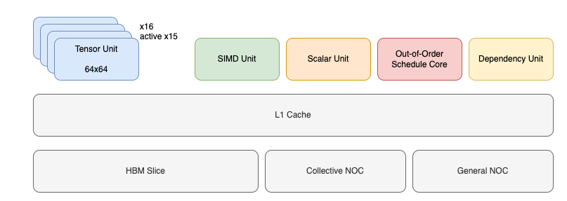
For all operations, as long as there is an idle Tensor Unit, the Out-of-Order Core can commit multiple times to raise instruction-level parallelism, while data dependencies are all determined by the L1 Cache state, and data can also be prefetched under hardware control. As for the size of the L1 Cache, we made a detailed evaluation along several dimensions — HBM bandwidth and latency, NOC interconnect bandwidth, and Tensor Unit processing capability — and estimate the L1 Cache size per Core Slice at 512KB. Compared with the Blackwell chip, the Blackwell chip in fact has several storage regions — RegisterFile / L1 Cache / SMEM / TMEM — whereas Jalapeño very cleanly handles it as one single region connected to the HBM Slice.
This is exactly Jalapeño's core decision: spend more die area on multiple Tensor Units, and strip out the complex Global L2 / scheduler as well as the multiple storage structures inside the SM. It then does not need to chase higher peak FLOPs but instead pays more attention to sustainable FLOPs in real work. And when some workloads are lighter, it can further power-gate some execution units off to obtain a higher Perf-Watt Ratio.
3.3 Memory Subsystem
The biggest change in the memory subsystem is the NUMA structure. Referring to some HBM4 data, a single HBM4 stack contains 64 pseudo-channels (PC) with a 32bit width and burst length = 8. We therefore infer the connection structure as follows
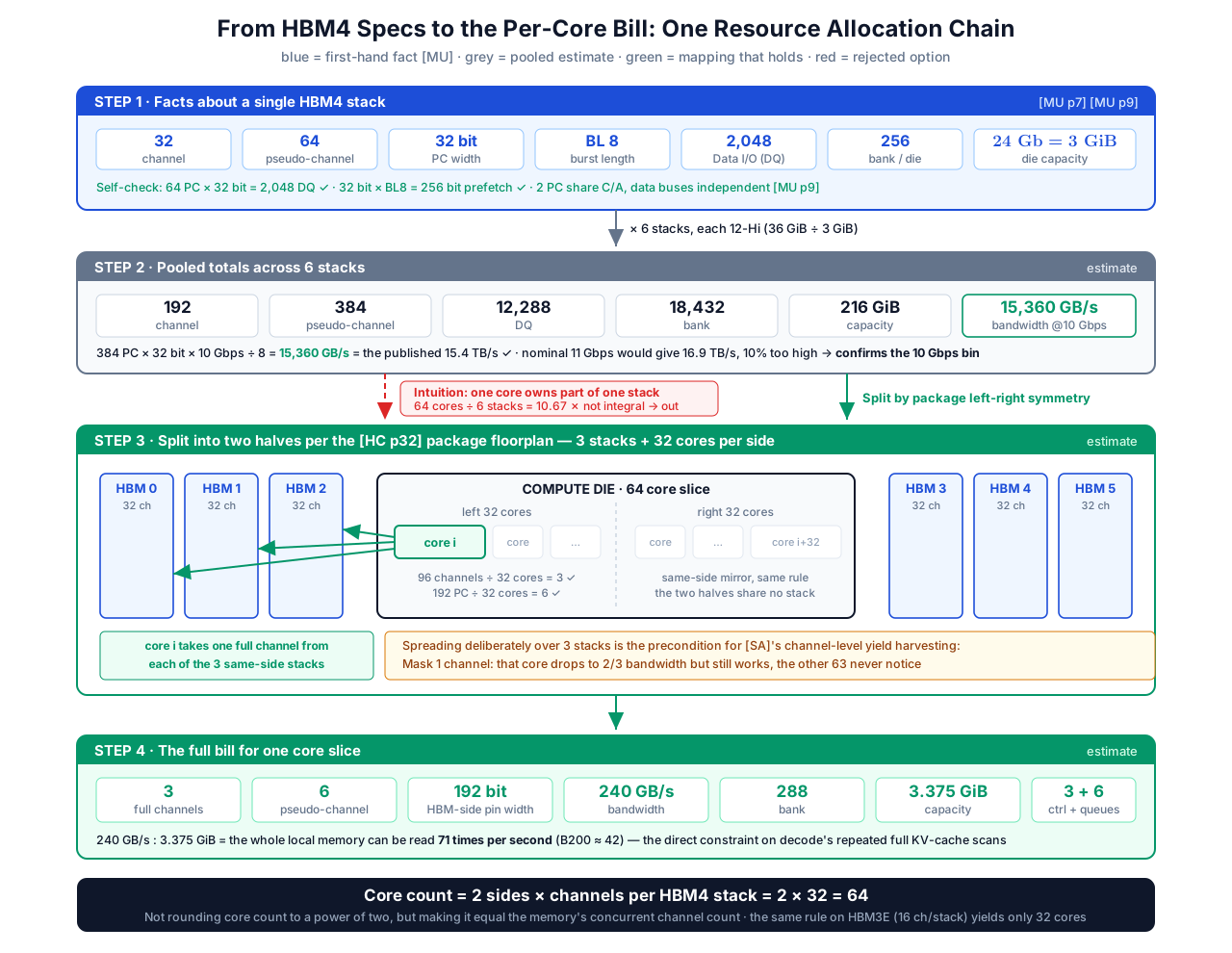
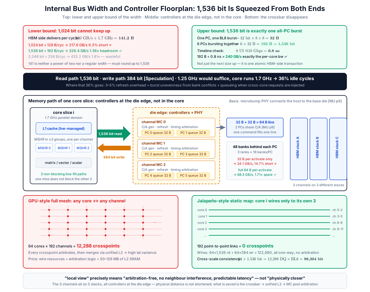
The width connected to a single Core Slice is 1536 bit, each Core Slice connects to three HBM stacks, and the total bandwidth is 240GB/s. We can see one benefit of such a design: compared with the unified memory access of a GPGPU, this approach can eliminate a great deal of jitter, and the latency is lower.
3.4 On-Chip Network
Overall, between each Core Slice and the HBM directly attached to it there is a Local view, which is mainly responsible for storing some KVCache slices and weight slices inside the Core; then, for the NUMA structure among multiple Cores, the whole NOC is divided into two parts, one dedicated to collective communication and the other a general-purpose NOC.
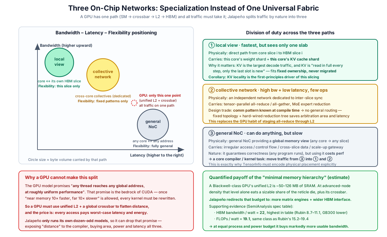
This is where the biggest difference from a GPU lies. A GPU's programming model dictates that any thread can access any global memory address arbitrarily — that is what the CUDA ecosystem dictates — but the speeds of different memory accesses differ enormously, and those differences need L2 to level out. Yet because of physical constraints, in Dual-Die architectures like Blackwell/Rubin the L2 has already been split into 4 pieces, and it too has large latency differences internally, so the whole system gets dragged down by large access latency. Jalapeño, by contrast, separates out this complexity of memory-access distance through the NUMA architecture: the chip becomes simpler, and the complexity of writing operators is handed to the compiler, while the compiler in turn, with the help of an LLM-Agent, can perform extreme performance optimization. So in the end, on the chip, Jalapeño obtains a triple benefit in area / power / latency.
We speculate that the General NOC is a small-bandwidth local Mesh + Global Switch architecture, and what is distinctive is the Collective Network. Let us unfold that a bit here: taking constraints such as latency into account, we simulated several topologies and ultimately concluded that it is an 8x8 2-stage architecture, with every 8 Core Slices forming a group and then a global reduction across the 8 groups.
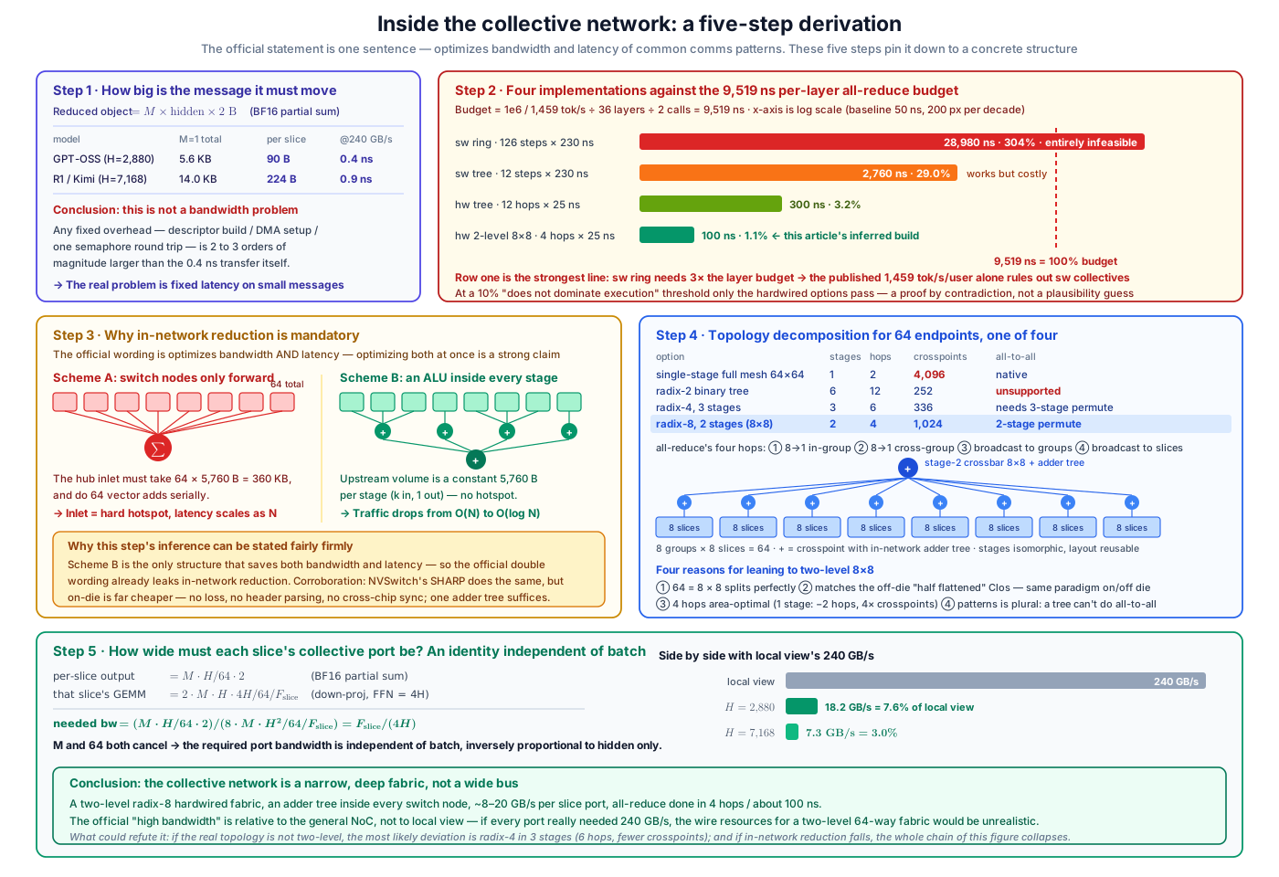
It needs to support all-reduce and all-gather / broadcast across 64 Core Slices, and connects directly to each Core Slice's L1. Overall, combined with the Core Slice's superscalar execution structure, it can build very fine-grained tile-based collectives, so the overall latency can be nicely hidden during GEMM computation and when fused with other operators.
3.5 System Architecture
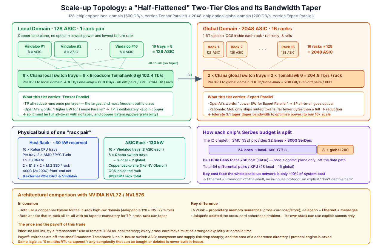
The whole system, similar to Alibaba's Panjiu AL128 super-node, adopts an architecture that separates the CPU-Tray from the Compute-Tray. OpenAI's CPU Tray (codename: Katsu) has 2x Turin X86 CPUs and 1.5TB of memory, while the Compute Tray (codename: Vindaloo) contains 8 Jalapeño ASICs, with the two interconnected over PCIe DAC. It then uses 2 sets of ScaleUP for interconnect, both using standard Ethernet solutions: the Local Domain ScaleUP supports 128 cards at 600GB/s of bandwidth, mainly used for TP parallelism, while the Global domain supports 2048 cards at 200GB/s of bandwidth
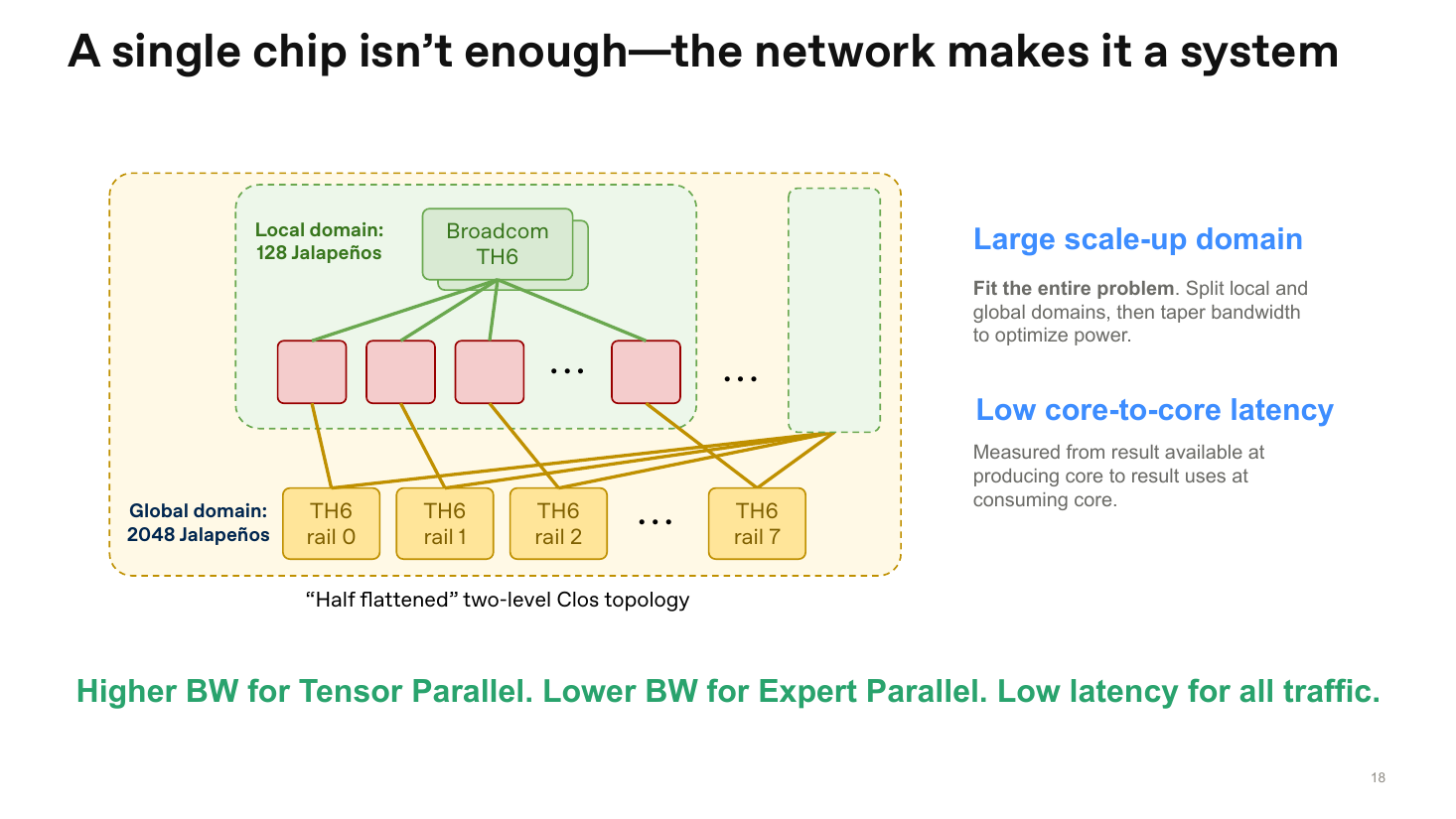
The Local Domain uses a Cable-Tray at the back to interconnect with the Switch-Tray (codename: Chana) over copper cables, while the Global Domain uses optical interconnect. The Switch-Tray uses the mature BRCM Tomahawk 6 102.4T Ethernet switch chip. Its choice of standard Ethernet gives it much less bandwidth than the Nvidia GPU's 1.8TB/s ScaleUP. But buying the switch directly as a Broadcom Tomahawk 6 commodity part, with no need to develop a switch ASIC in-house, saves a project that has to tape out in 9 months not just design effort but an entire class of risk — supply-chain and ecosystem risk drop substantially. This is also the very reason I started working on Ethernet ScaleUP (NetDAM) back in 2020.
The whole rack architecture is shown in the figure on the right below:
On the left side sit the CPU servers, 16 of them in total in a 2U form factor; the cables crossing between racks in the middle are the PCIe DAC Cables, 8 per CPU server in total, presumably using a PCIe Gen5x8 structure to connect to the Compute-Tray — or else there are two PCIe Switch chips inside the Compute-Tray, with the CPU connected to the PCIe Switch over 4x PCIe-Gen5x16. On the right, 8 Compute-Trays are placed at the top and 8 at the bottom, and in the middle are 6 1U Switch-Trays for the Local Domain, each Switch Tray holding 1 TH6; the one used for the Global Domain uses a 2U chassis. SemiAnalysis believes this contains 2 TH6 switch chips, but if I were designing it, this spot would probably mainly hold some Shuffle boxes or some small OCS / retimers plus the components that power and cool the optical modules, and the Global Domain switches would be placed in a separate rack, because it is a Rail-based topology.
The whole design is very thoroughly considered: TP is handled in the Local Domain, and EP uses the lower-bandwidth Global Domain. And for Jalapeño there is no need, as with Nvidia, to accumulate a very large Batch to do EP, so the synchronization cost is relatively lower.
4. Software Architecture
The core difficulty of a traditional compiler is predicting performance in the absence of real measurements, which forces you to construct a cost model. The accuracy of the cost model determines the compiler's ceiling, and on a machine that has caches, out-of-order execution, and on-chip network contention, the accuracy ceiling of a cost model is very low. Jalapeño's software stack gives up prediction. It turns the mapping decision into a measurable search problem: generate candidates → run them on chilisim or on real silicon → get real numbers → iterate.
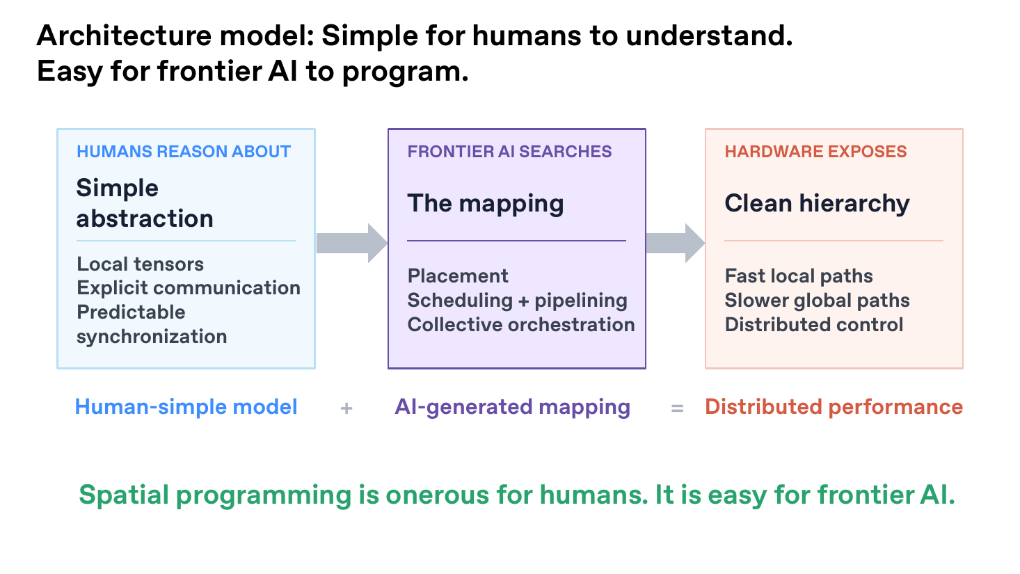
This is the biggest difference between it and traditional GPU chips: it fully leverages the capability of modern LLM-Agents to build the entire software system. This is exactly the sentence OpenAI emphasized: Spatial programming is onerous for humans. It is easy for frontier AI.
The whole system is structured in two layers. Lowering uses Gluon together with the Linear Layouts algebra (for a detailed analysis see Learning a Bit About Linear Layout). Mapping to the hardware then uses LLM-Agents much more heavily for search and tuning.
| Layer | Responsibility | How decisions are made | Correctness guarantee |
|---|---|---|---|
| Lowering layer | Gluon → machine code, layout transformation, swizzle derivation | Analytic solving, deterministic | Linear Layouts algebra |
| Mapping layer | Placement / pipeline scheduling / collective communication orchestration | Search, driven by AI | Relies on executable tests + e2e validation |
The whole publicly disclosed software stack is then divided into six layers:
| Layer | Component | Responsibility | Approximate CUDA-stack counterpart |
|---|---|---|---|
| L5 Serving | Teacup | Request scheduling, batch assembly, KV management, speculative decoding orchestration | vLLM / SGLang / TensorRT-LLM |
| L4 Execution body | gigakernel | One giant kernel resident on chip, containing the complete decode loop internally | persistent kernel + CUDA Graph |
| L3 Kernel language | Gluon | A low-level tile SPMD kernel language of the Triton family | Abstraction level close to CuTe / CUTLASS; the frontend and toolchain are Triton |
| L2 Layout algebra | Linear Layouts + TensorInfo | An algebraic representation of tensor layout; TensorInfo encodes both layout and physical placement | CuTe Layout (layout only, no placement) |
| L1 Low level | Assembly-like kernels (~3000 lines) + in-house sanitizer | The innermost layer, hand-written / AI-written; race and out-of-bounds checking | PTX/SASS + compute-sanitizer |
| L0 Measurement | chilisim | Cycle-accurate simulator, < 5% error against real silicon | Nsight Compute (profiling only, not prediction) |
The detailed process of the whole framework is summarized as follows:
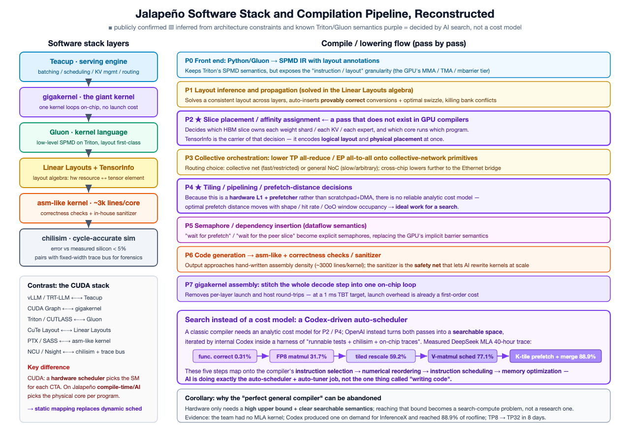
This figure draws Jalapeño's software-stack layering together with the compilation Pass pipeline derived in this article; read the legend first: solid blocks are publicly confirmed, hatched ones are inferred from architectural constraints and known Triton/Gluon semantics, and purple ones are decided by AI search rather than by a cost model.
The layering on the left (Teacup / gigakernel / Gluon / Linear Layouts + TensorInfo / ~3000 lines of assembly-like kernels / chilisim) gives an approximate CUDA-stack counterpart for every layer (vLLM ↔ Teacup, CUDA Graph ↔ gigakernel, CuTe ↔ Linear Layouts, PTX/SASS ↔ assembly-like, NCU ↔ chilisim), but there is only one key difference: in the CUDA stack the hardware scheduler decides which SM a CTA lands on, whereas here compile time / AI decides which physical core a program lands on — that is, static spatial mapping replaces dynamic scheduling.
In the P0–P7 Pass flow on the right, the two marked with ★ (P2 slice placement / affinity assignment, P4 tiling / pipelining / prefetch distance) simply do not exist in a GPU compiler: P2 decides which HBM slice every weight shard, every KV, and every expert belongs to, and TensorInfo is precisely the carrier of this decision, encoding both the logical layout and the physical placement; P4, on the other hand, is naturally suited to being handed to search because "hardware L1 + prefetch" has no reliable analytic cost model (the optimal prefetch distance varies with shape / hit rate / OoO window occupancy).
The 40-hour measured curve for DeepSeek MLA at the bottom is the hardest evidence in the whole chapter: functionally correct 0.31% → FP8 matrices 31.7% → blocked look-ahead rescaling 59.2% → V-matmul scheduling 77.1% → K-tile prefetch + coalesced memory access 88.9%. These five steps correspond in order to a traditional compiler's instruction selection → numerical algorithm reordering → instruction scheduling → memory-access optimization — what the AI is doing is the job of an auto-scheduler + auto-tuner.
The corollary at the end of the figure answers "why it is possible to give up a general-purpose compiler": the hardware only needs to guarantee that the upper bound is high enough and that the semantics are clear enough to be searchable, and then finding the path that reaches that upper bound turns from "a compiler research problem" into "a search compute problem".
This is also why I was trying that Anthropic VLIW+SIMD interview problem a while ago — not to look for a job, of course, but to gain a deeper understanding of the whole optimization flow.
I also used some AI tools to do a detailed analysis of the Gluon code; the specific analysis will not be made public.. the figure below is a rough process analysis
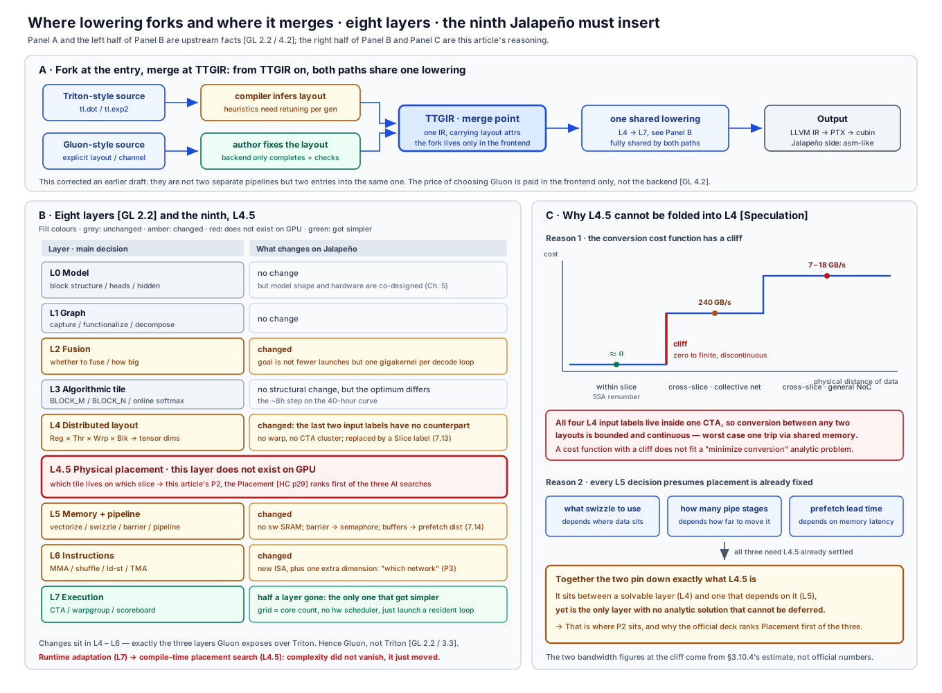
On another front, we need to pay attention to how Gluon and XLS work together; this is an excellent reference for hardware/software co-design, and we will unfold a detailed analysis in the next chapter
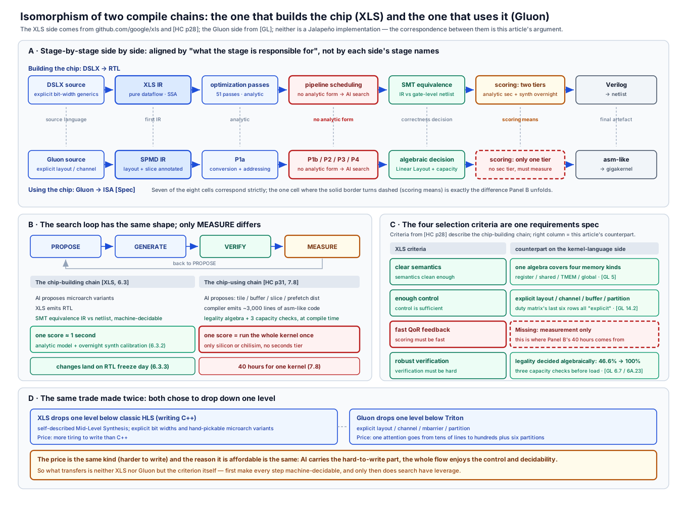
5. Chip Design
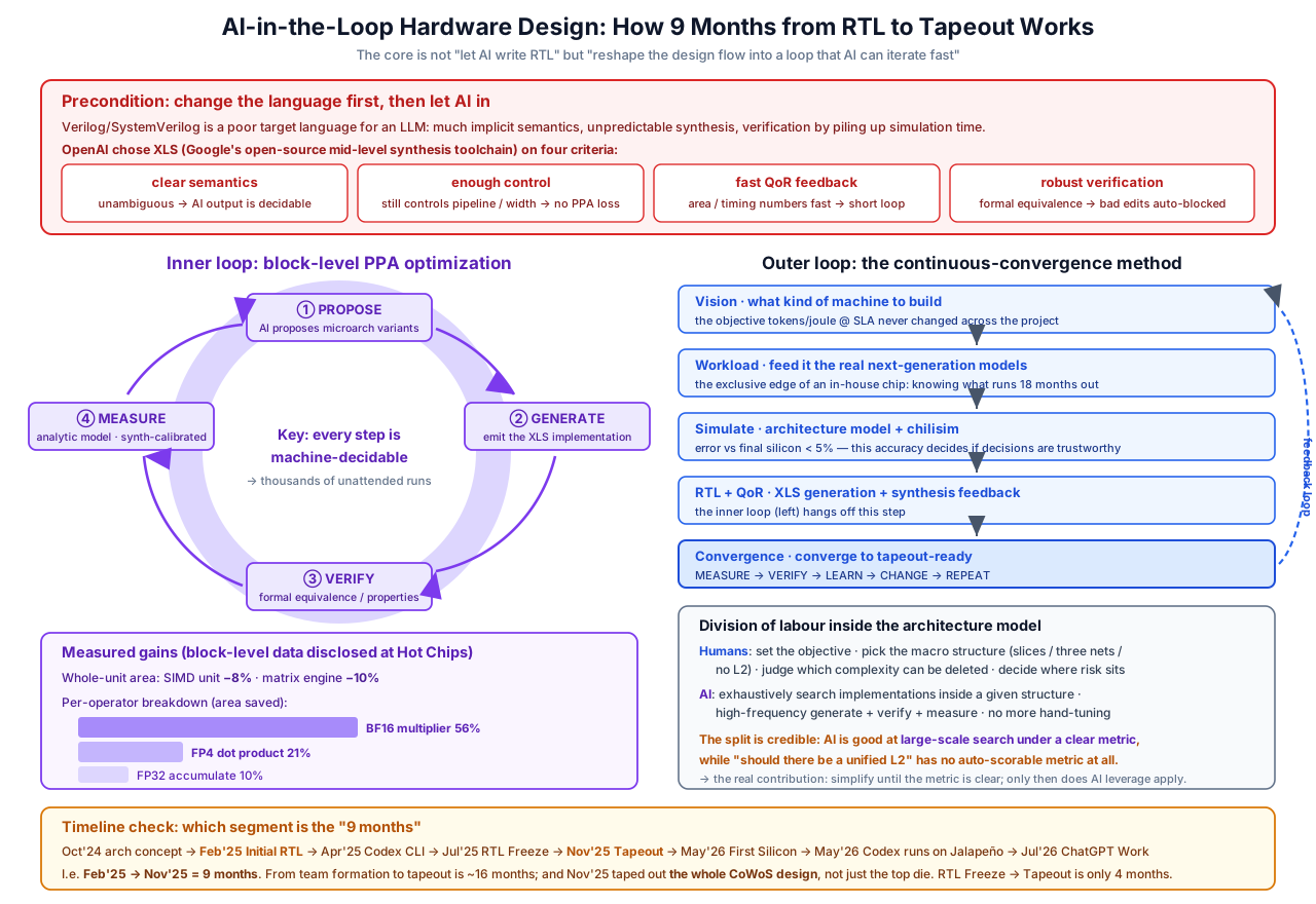
The whole project took only 9 months from the first line of RTL to tapeout, which basically completely overturns the existing chip development flow; this is also a direction I have been paying very close attention to for quite a long time recently.
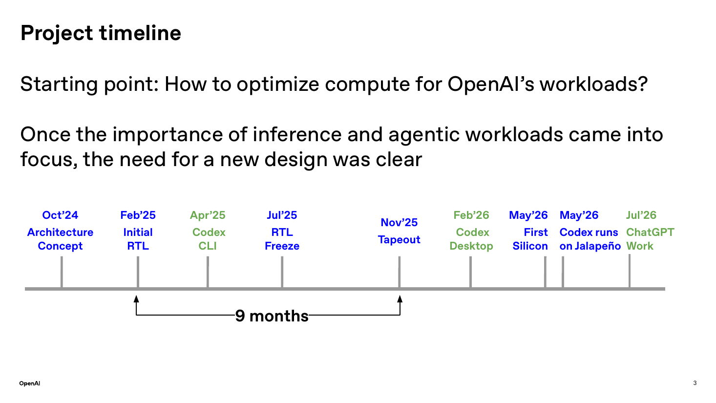
5.1 The Key Prerequisite: Change the Language First, Then Let AI Take the Stage
The key prerequisite of the whole design is: change the language first, then let AI take the stage
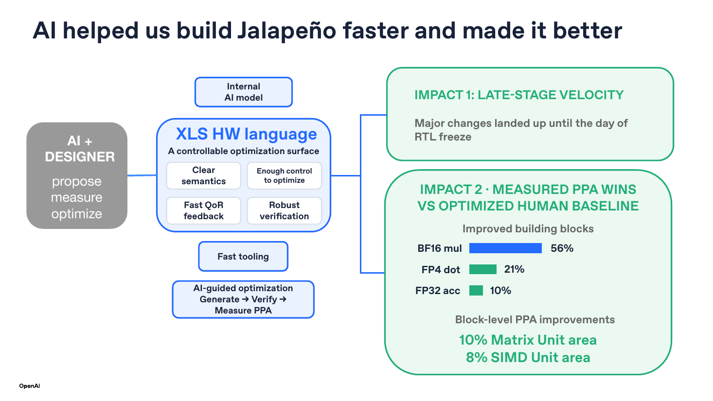
Note that the layout of this slide is itself the argument: AI + DESIGNER, Internal AI model, and Fast tooling all point with arrows at the blue XLS HW language in the middle. In other words, in OpenAI's own narrative, XLS is the substrate on which the AI and the designer act jointly. We note that XLS positions itself as:
XLS is a 'Mid-Level' Synthesis toolchain for hardware development. It is similar and has some of the same goals as High-level Synthesis (HLS) tools however it operates at a generally lower level.
| Criterion | Why it is necessary for "letting AI step in" |
|---|---|
| clear semantics | Unambiguous semantics → the behavior of AI-generated code is decidable; you will not run into "what got synthesized does not match simulation", the kind of problem an AI cannot self-check |
| enough control | Still able to control down to pipeline stage and bit width → does not sacrifice the PPA ceiling, otherwise the ceiling of AI optimization would be capped by the language itself |
| fast QoR feedback | Quickly getting area/timing numbers → a short closed-loop cycle is the prerequisite for search to be viable |
| robust verification | Formal equivalence is decidable → an AI's wrong change can be automatically blocked, without needing a human to review every change |
What these four have in common is: make every step machine-decidable. This is what turns "design" from a process requiring human judgment into a search problem that can be scored automatically. We speculate the whole process is as follows:
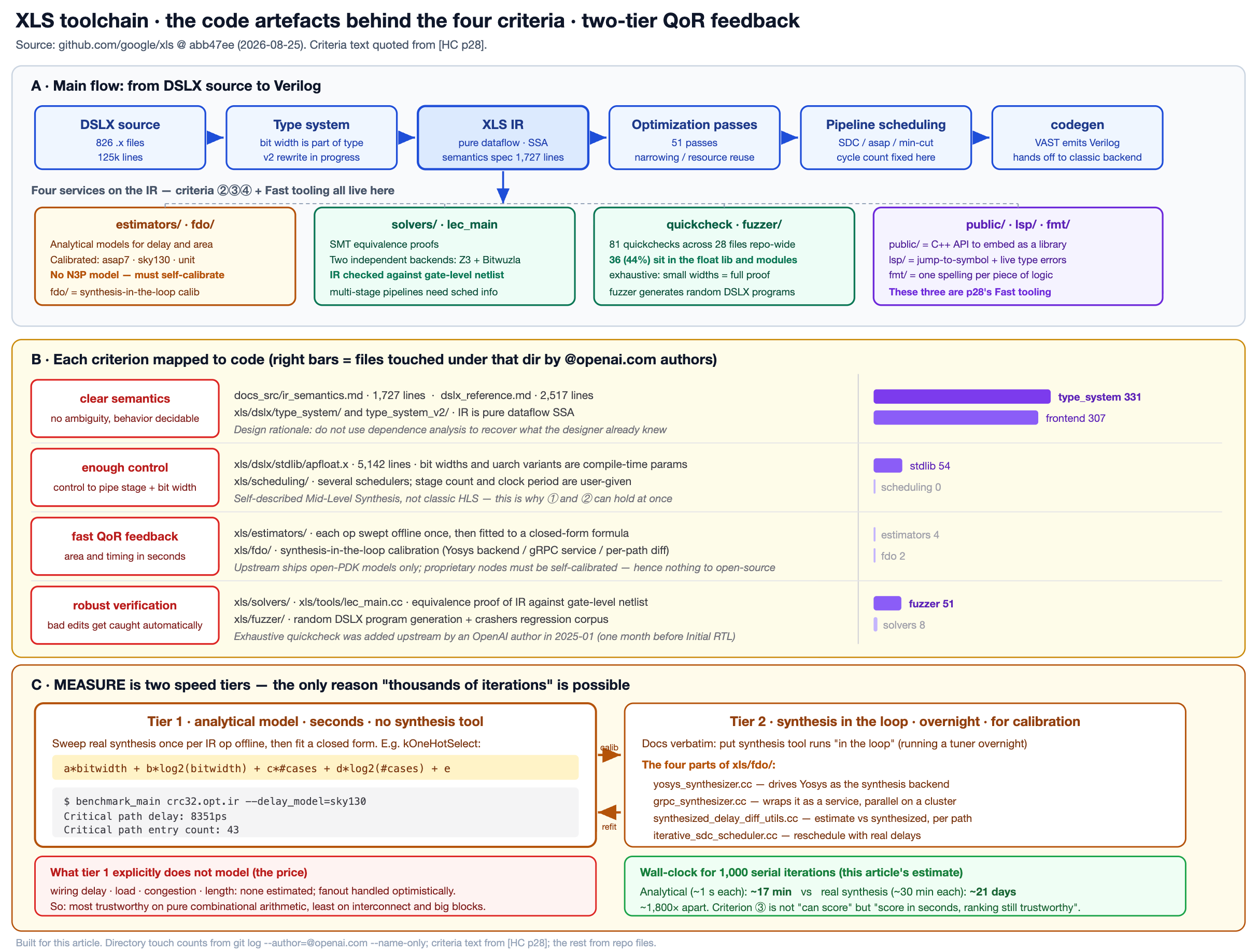
5.2 How the Design Closes the Loop
OpenAI's Hotchips presentation material is as follows:
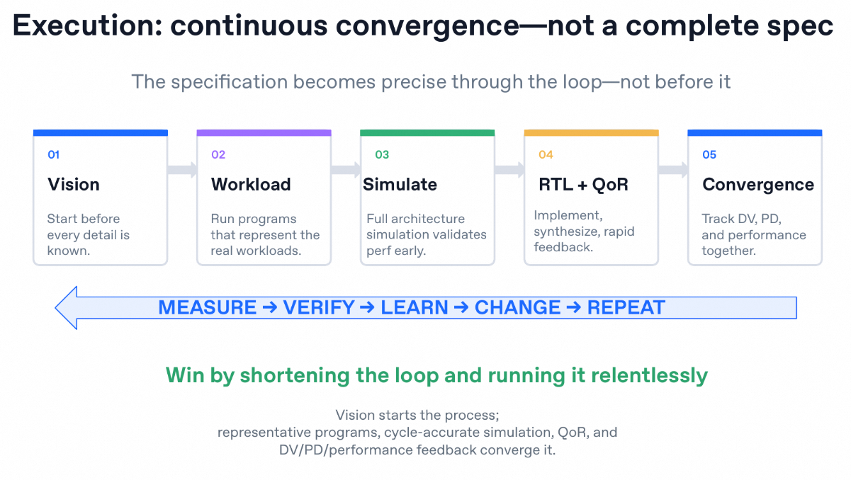
The most critical part of it is the division of labor between human and machine. Humans are responsible for defining some objective functions, choosing the main structure of the whole chip, judging which architectural complexities can be deleted, and planning the macro architecture of the whole hardware/software co-design. The AI is responsible for detailed, high-frequency exhaustive search within that structure, freeing engineers from the work of manually tuning area/timing. The boundary of the division of labor is let the AI take charge of what it is good at — large-scale search under clear criteria — rather than generating code for macro-level system architecture where there is no clear objective to judge against.
6. Looking Ahead
6.1 A Comparison with the Nvidia GPGPU Architecture
Let us make a complete comparison between it and the Nvidia GPGPU:
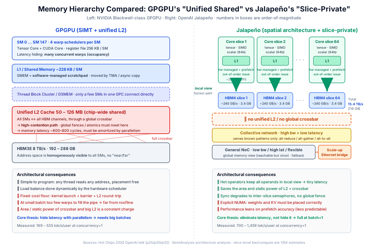
A GPU's storage hierarchy is registers → L1/SMEM → (Cluster/DSMEM) → unified L2 (50–126 MB) → HBM, where the unified L2 is shared by the whole chip and all SMs access all HBM channels through a global crossbar.
Also very much worth comparing is the architecture of their Tensor Units
| Dimension | The 5th-generation Tensor Core in a B300 SM | The matrix array in a Jalapeño slice |
|---|---|---|
| FP4 MACs per unit | 4,096 / TC × 4 TC | 4,096 / array × 16 arrays |
| Unit count and yield harvesting | 80 SMs physical, 74 enabled | 16 arrays physical, 15 enabled |
| Where the accumulator lives | TMEM, 128 rows × 512 cols (256 KB/SM) | 64 FP32 columns inside the array |
| Issue model | Single-thread lane-0 async + mbarrier completion notification | Statically orchestrated at compile time |
| Physical caliber of the K dimension | K × sizeof = 32 B constant | Same (reduction depth set by the side length) |
| Granularity of the M dimension | 64, and M<64 is illegal under 1 CTA |
Can go as fine as 1 in the row direction |
| Reduction structure | Inside the array, not disclosed | Broadcast + adder tree, 6–9 cyc |
A detailed comparison was made:
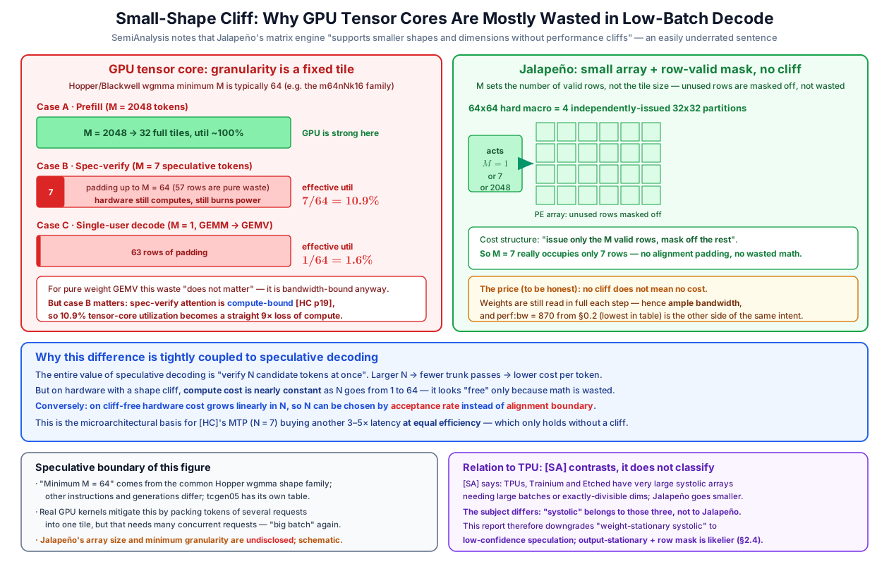
In terms of die area, Jalapeño uses more tensor units, with an estimated area of 180 mm² accounting for 22% of the whole Die area, and does not use a large L2 Cache or a complex RF/SMEM/TMEM/L1Cache memory hierarchy.
Jalapeño cuts the cores and the HBM into 64 slices, and each core slice has a low-latency local view of its own share of HBM; synchronization between slices goes over a dedicated high-bandwidth collective communication network; and there is another general-purpose NoC responsible for odd jobs and for reaching the scale-up network. Officially this is called a "minimal memory hierarchy", and they explicitly state that relative to a GPU's complex memory system this is an enormous advantage.
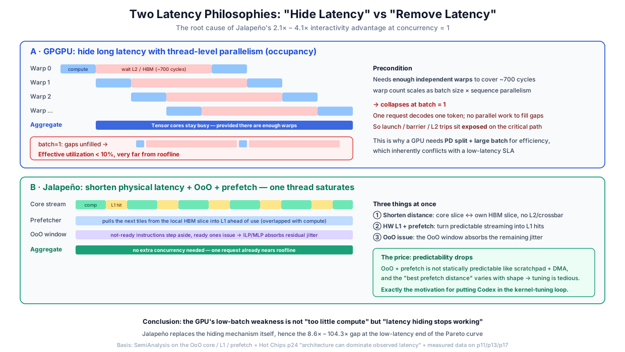
Also, the two system designs represent two different lines of thinking. The Nvidia GPGPU obtains higher throughput through higher Occupancy and latency hiding, which is very effective for training scenarios, but for inference with small batches and strict SLA requirements this approach is not suitable. Jalapeño, by contrast, eliminates latency directly with "shorten the distance + prefetch + out-of-order window", without relying on concurrency.
On another front, within each layer of a Transformer, the attention output has to be merged across heads and the MLP output has to be summed across the hidden dimension. Once these dimensions are cut across multiple execution units (on-die slices or cross-die TP), every layer needs at least one reduction. The layer count is given by the model structure, so the number of reductions is given as well:
The first term falls linearly with the degree of parallelism; the second does not fall with the degree of parallelism, and usually even rises with it, because you have to cross a farther domain. The NOC design therefore also takes this effect into account: if this latency overhead can be reduced significantly, then we can more effectively increase the scale of TP parallelism.
A comparison of the two architectures follows:
| GPU | Jalapeño | |
|---|---|---|
| Mechanism | Temporal multiplexing: cover memory latency with a large number of concurrent warps | Shorten the distance + prefetch + out-of-order window |
| What it depends on | Enough independent work (i.e. a large enough batch) | Instruction-level parallelism within a single instruction stream |
| At batch = 1 | Not enough schedulable warps, the pipeline idles, the mechanism breaks down | The mechanism is unchanged — it never depended on concurrency in the first place |
| Measured (single-concurrency tok/s/user) | 169 – 535 | 700 – 1,459 |
6.2 OpenAI's Roadmap
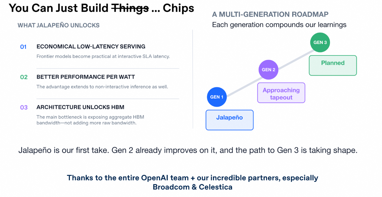
With the collaboration of LLM-Agents, OpenAI claims that after the whole chip (A0) came back from the fab and went through further optimization, B0 — estimated to have another 25% performance uplift — has already been sent to tapeout, and that the second generation in the future will support training
6.3 Some Concluding Analysis
Overall, earlier this year I already noticed this enormous opportunity of LLM-Agent and chip co-design. From using an LLM-Agent to reverse-engineer Blackwell's architecture in detail, to getting to third place in the Anthropic VLIW+SIMD challenge with my own hands, I have basically fully mastered the whole iteration flow. A few months ago the chip architecture was also basically sorted out, and the basic judgment is consistent with OpenAI's — which is exactly what I mentioned last year when I was analyzing the Blackwell architecture, in that article Jensen forwarded internally at the company: the existing warp scheduling mechanism absolutely must be changed in order to get a several-fold improvement in Perf-Watt Ratio.
As for interconnect, that has always been what I am best at: from the world-leading Ethernet Based ScaleUP implementation starting in 2020, to now comprehensively surpassing Nvidia in the DPU/NIC field, and in the next generation the DPU/NIC will also have a crushing advantage over Nvidia in PPA — just like Jalapeño's several-fold to several-tens-of-fold improvement. By then, whether in ScaleUP/ScaleOut, there will not be many players who can go toe-to-toe with us, and now the compute chip is basically ready as far as how to do it...
[1] Challenges and Research Directions for Large Language Model Inference Hardware: https://arxiv.org/abs/2601.05047
[2] Dissecting SM_120 through Microbenchmarking: https://zartbot.github.io/micro_arch/nvidia/sm_120/index.html